HIP4020

Features: • Two Independent Controlled Complementary MOS Power Output Half H-Drivers (Full-Bridge) for Nominal 3V to 12V Power Supply Operation• Split ±Voltage Power Supply Option for Output Drivers• Load Switching Capabilities to 0.5A• Single Supply Range +2.5V to +15VR...

product image

HIP4020 Picture
SeekIC No. : 004362693 Detail

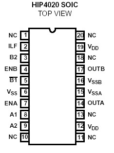
HIP4020: Features: • Two Independent Controlled Complementary MOS Power Output Half H-Drivers (Full-Bridge) for Nominal 3V to 12V Power Supply Operation• Split ±Voltage Power Supply Option for Ou...

floor Price/Ceiling Price
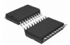
Part Number:
HIP4020
Supply Ability:
5000

Price Break

  • Qty
  • 1~5000
  • Unit Price
  • Negotiable
  • Processing time
  • 15 Days
Total Cost: $ 0.00

SeekIC Buyer Protection PLUS - newly updated for 2013!

  • Escrow Protection.
  • Guaranteed refunds.
  • Secure payments.
  • Learn more >>

Month Sales

268 Transactions

Rating

evaluate  (4.8 stars)

Upload time: 2024/4/26

Payment Methods

All payment methods are secure and covered by SeekIC Buyer Protection PLUS.

Notice: When you place an order, your payment is made to SeekIC and not to your seller. SeekIC only pays the seller after confirming you have received your order. We will also never share your payment details with your seller.
Product Details

Description


Features:

• Two Independent Controlled Complementary MOS Power Output Half H-Drivers (Full-Bridge) for Nominal 3V to 12V Power Supply Operation
• Split ±Voltage Power Supply Option for Output Drivers
• Load Switching Capabilities to 0.5A
• Single Supply Range +2.5V to +15V
• Low Standby Current
• CMOS/TTL Compatible Input Logic
• Over-Temperature Shutdown Protection
• Over-Current Limit Protection
• Over-Current Fault Flag Output
• Direction, Braking and PWM Control


Application

• DC Motor Driver
• Relay and Solenoid Drivers
• Stepper Motor Controller
• Air Core Gauge Instrument Driver
• Speedometer Displays
• Tachometer Displays
• Remote Power Switch
• Battery Operated Switch Circuits
• Logic and Microcontroller Operated Switch


Pinout

  Connection Diagram


Specifications

Supply Voltage; VDD to VSS or VSSA or VSSB . . . . . . . . . . . . . .+15V
Neg. Output Supply Voltage, (VSSA, VSSB). . . . . . . . . . . . . (Note 1)
DC Logic Input Voltage (Each Input) . . . (VSS -0.5V) to (VDD +0.5V)
DC Logic Input Current (Each Input) . . . . . . . . . . . . . . . . . .±15mA
ILF Fault Output Current . . . . . . . . . . . . . . . . . . . . . . . . . . .±15mA
Output Load Current, (Self Limiting, See Elec. Spec.). . . ±IO(LIMIT)


Description

In the Functional Block Diagram of the HIP4020, the four switches and a load are arranged in an H-Configuration so that the drive voltage from terminals OUTA and OUTB can be cross-switched to change the direction of current flow in the load. HIP4020 is commonly known as 4-quadrant load control. As shown in the Block Diagram of HIP4020, switches Q1 and Q4 are conducting or in an ON state when current flows from VDD through Q1 to the load, and then through Q4 to terminal VSSB; where load terminal OUTA is at a positive potential with respect to OUTB. Switches Q1 and Q4 are operated synchronously by the control logic. The control logic switches Q3 and Q2 to an open or OFF state when Q1 and Q4 are switched ON. To reverse the current flow in the load, the switch states are reversed where Q1 and Q4 are OFF while Q2 and Q3 are ON. Consequently, current then flows from VDD through Q3, through the load, and through Q2 to terminal VSSA, and load terminal OUTB is then at a positive potential with respect to OUTA. Terminals ENA and ENB are ENABLE Inputs for the Logic A and B Input Controls. The ILF output of HIP4020 is an Over-Current Limit Fault Flag Output and indicates a fault condition for either Output A or B or both. The VDD and VSS are the Power Supply reference terminals for the A and B Control Logic Inputs and ILF Output. While the VDD positive power supply terminal is internally connected to each bridge driver, the VSSA and VSSB Power Supply terminals are separate and independent from VSS and may be more negative than the VSS ground reference terminal. The use of level shifters in the gate drive circuitry to the NMOS (low-side) output stages allows controlled level shifting of the output drive relative to ground.


Customers Who Bought This Item Also Bought

Margin,quality,low-cost products with low minimum orders. Secure your online payments with SeekIC Buyer Protection.
Connectors, Interconnects
RF and RFID
Motors, Solenoids, Driver Boards/Modules
Inductors, Coils, Chokes
Fans, Thermal Management
View more