HM67S36130

Features: · 3.3V ± 5% Operation· LVCMOS Compatible Input and Output· Synchronous Operation· Internal self-timed Late Write· Asynchronous G Output Control· Byte Write Control (4 byte write selects, one for each 9 bits)· Power down mode is provided· Differential PECL Clock Inputs· Boundary Scan· Pro...

product image

HM67S36130 Picture
SeekIC No. : 004363616 Detail

HM67S36130: Features: · 3.3V ± 5% Operation· LVCMOS Compatible Input and Output· Synchronous Operation· Internal self-timed Late Write· Asynchronous G Output Control· Byte Write Control (4 byte write selects, o...

floor Price/Ceiling Price

Part Number:
HM67S36130
Supply Ability:
5000

Price Break

  • Qty
  • 1~5000
  • Unit Price
  • Negotiable
  • Processing time
  • 15 Days
Total Cost: $ 0.00

SeekIC Buyer Protection PLUS - newly updated for 2013!

  • Escrow Protection.
  • Guaranteed refunds.
  • Secure payments.
  • Learn more >>

Month Sales

268 Transactions

Rating

evaluate  (4.8 stars)

Upload time: 2024/4/18

Payment Methods

All payment methods are secure and covered by SeekIC Buyer Protection PLUS.

Notice: When you place an order, your payment is made to SeekIC and not to your seller. SeekIC only pays the seller after confirming you have received your order. We will also never share your payment details with your seller.
Product Details

Description


Features:

·  3.3V ± 5% Operation
·  LVCMOS Compatible Input and Output
·  Synchronous Operation
·  Internal self-timed Late Write
·  Asynchronous G Output Control
·  Byte Write Control
     (4 byte write selects, one for each 9 bits)
·  Power down mode is provided
·  Differential PECL Clock Inputs
·  Boundary Scan
·  Protocol Single Clock Register-Latch Mode


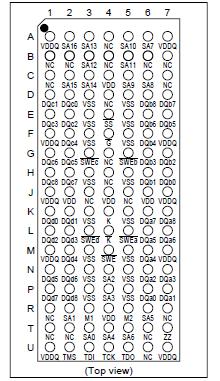
Pinout

  Connection Diagram


Specifications

Parameter
Symbol
Value
Unit
Note
supply voltage
VDD
0.5 to + 4.6
V
1
Output Supply Voltage
VDDQ
0.5 to VDD+0.5
V
1, 4
Voltage on any pin
VIN
0.5 to VDD+0.5
V
1, 4
Operating Temperature
Ta
0 to 70 (Tj max = 110)
°C
Storage Temperature
ToprTstg (bias)
55 to 125
°C
Input Latchup Current
ILI
±200
mA
Output Current per pin
Iout
±25
mA

Notes: 1. All voltage are referenced to VSS.
2. Permanent device damage may occur if Absolute Maximum Ratings are exceeded. Functional
operation should be restricted the Operation Conditions. Exposure to higher than recommended
voltages for extended periods of time could affect device reliability.
3. These Bi-CMOS memory circuits have been designed to meet the DC and AC specifications
shown in the tables after thermal equilibrium has been established.
4. Not exceed 4.6 V
5. Power Up Initialization
The following supply voltage application sequence is recommended: VSS, VDD then VDDQ.
Remember according to the Absolute Maximum Ratings table, VDDQ is not to exceed VDD + 0.5 V,
whatever the instantaneous value of VDD.


Customers Who Bought This Item Also Bought

Margin,quality,low-cost products with low minimum orders. Secure your online payments with SeekIC Buyer Protection.
Inductors, Coils, Chokes
Cable Assemblies
Industrial Controls, Meters
Fans, Thermal Management
Motors, Solenoids, Driver Boards/Modules
View more