HY5DS283222BF

Features: The Hynix HY5DS283222BF(P) guarantee until 166MHz speed at DLL_off condition1.8V VDD and VDDQ wide range max power supply supportsAll inputs and outputs are compatible with SSTL_2 nterface12mm x 12mm, 144ball FBGA with 0.8mm pin pitchFully differential clock inputs (CK, /CK) operationDo...

product image

HY5DS283222BF Picture
SeekIC No. : 004368272 Detail

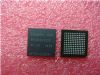
HY5DS283222BF: Features: The Hynix HY5DS283222BF(P) guarantee until 166MHz speed at DLL_off condition1.8V VDD and VDDQ wide range max power supply supportsAll inputs and outputs are compatible with SSTL_2 nterfac...

floor Price/Ceiling Price

Part Number:
HY5DS283222BF
Supply Ability:
5000

Price Break

  • Qty
  • 1~5000
  • Unit Price
  • Negotiable
  • Processing time
  • 15 Days
Total Cost: $ 0.00

SeekIC Buyer Protection PLUS - newly updated for 2013!

  • Escrow Protection.
  • Guaranteed refunds.
  • Secure payments.
  • Learn more >>

Month Sales

268 Transactions

Rating

evaluate  (4.8 stars)

Upload time: 2024/4/26

Payment Methods

All payment methods are secure and covered by SeekIC Buyer Protection PLUS.

Notice: When you place an order, your payment is made to SeekIC and not to your seller. SeekIC only pays the seller after confirming you have received your order. We will also never share your payment details with your seller.
Product Details

Description


Features:

The Hynix HY5DS283222BF(P) guarantee until
166MHz speed at DLL_off condition
1.8V VDD and VDDQ wide range max power supply supports
All inputs and outputs are compatible with SSTL_2 nterface
12mm x 12mm, 144ball FBGA with 0.8mm pin pitch
Fully differential clock inputs (CK, /CK) operation
Double data rate interface
Source synchronous - data transaction aligned to
bidirectional data strobe (DQS0 ~ DQS3)
Data outputs on DQS edges when read (edged DQ)
Data inputs on DQS centers when write (centered DQ)
Data(DQ) and Write masks(DM) latched on the both
rising and falling edges of the data strobe
All addresses and control inputs except Data, Data
strobes and Data masks latched on the rising edges of the clock
Write mask byte controls by DM (DM0 ~ DM3)
Programmable /CAS Latency 5 / 4 supported
Programmable Burst Length 2 / 4 / 8 with both
sequential and interleave mode
Internal 4 bank operations with single pulsed /RAS
tRAS Lock-Out function supported
Auto refresh and self refresh supported 4096 refresh cycles / 32ms
Half strength and Matched Impedance driver option controlled by EMRS


Pinout

  Connection Diagram


Specifications

Parameter Symbol Rating Unit
Ambient Temperature

TA

0 ~ 70

oC
Storage Temperature TSTG -55 ~ 125 oC
Voltage on Any Pin relative to VSS VIN, VOUT -0.5 ~ 3.6 V
Voltage on VDD relative to VSS VDD -0.5 ~ 3.6 V
Voltage on VDDQ relative to VSS VDDQ -0.5 ~ 3.6 V
Output Short Circuit Current IOS 50 mA
Power Dissipation PD 2 W
Soldering Temperature . Time TSOLDER 260 . 10 oC . sec


Description

The Hynix HY5DS283222 is a 134,217,728-bit CMOS Double Data Rate(DDR) Synchronous DRAM, ideally suited for the point-to-point applications which requires high bandwidth.

The Hynix 4Mx32 DDR SDRAMs HY5DS283222BF offer fully synchronous operations referenced to both rising and falling edges of the clock. While all addresses and control inputs are latched on the rising edges of the CK (falling edges of the /CK), Data, Data strobes and Write data masks inputs are sampled on both rising and falling edges of it. The data paths are inter- nally pipelined and 2-bit prefetched to achieve very high bandwidth. All input and output voltage levels are compatible with SSTL_2.


Customers Who Bought This Item Also Bought

Margin,quality,low-cost products with low minimum orders. Secure your online payments with SeekIC Buyer Protection.
Potentiometers, Variable Resistors
Circuit Protection
RF and RFID
Boxes, Enclosures, Racks
Inductors, Coils, Chokes
View more