DescriptionThe Hynix HY5DU561622FTP-5 series is a 268,435,456-bit CMOS double data rate(DDR) synchronous DRAM,ideally suited for the point-to-point applications which requires high bandwidth.The Hynix 16Mx16 DDR SDRAMs offer fully synchronous operations referenced to both rising and falling edges of the clock. While all addresses and control inputs are latched on the rising edges of the CK (falling edges of the /CK), Data,Data strobes and Write data masks inputs are sampled on both rising and falling edges of it. The data paths are internally pipelined and 2-bit prefetched to achieve very high bandwidth. All input and output voltage levels are compatible with SSTL_2.
Features of the HY5DU561622FTP-5 are:(1)JEDEC standard 400mil 66pin TSOP-II with 0.65mm pin pitch; (2)fully differential clock inputs (CK, /CK) operation; (3)double data rate interface; (4)source synchronous-data transaction aligned to bidirectional data strobe (DQS); (5)all addresses and control inputs except data, data strobes and data masks latched on the rising edges of the clock; (6)write mask byte controls by LDM and UDM; (7)internal 4 bank operations with single pulsed /RAS; (8)tRAS Lock-Out function supported; (9)auto refresh and self refresh supported.
The absolute maximum ratings of the HY5DU561622FTP-5 can be summarized as:(1)ambient temperature Ta:0 ~ 70; (2)storage temperature Tstg:-55 ~ 125; (3)voltage on any pin relative to Vss vin, vout:-0.5 ~ 3.6 V; (4)voltage on Vdd relative to Vss Vdd:-0.5 ~ 3.6V; (5)voltage on VddQ relative to Vss VddQ:-0.5 ~ 3.6 v; (6)output short circuit current Ios 50 mA; (7)power dissipation Pd:1w; (8)soldering temperature time Tsolder:260.10 .sec. Operational procedures other than those specified may result in undefined operation. Except for CKE, inputs are not recognized as valid until after VREF is applied. CKE is an SSTL_2 input, but will detect an LVCMOS LOW level after VDD is applied. Maintaining an LVCMOS LOW level on CKE during power-up is required to guarantee that the DQ and DQS outputs will be in the High-Z state,where they will remain until driven in normal operation (by a read access). After all power supply and reference voltages are stable, and the clock is stable, the DDR SDRAM requires a 200us delay prior to applying an executable command.

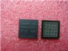
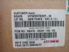
 HY5DU561622FTP-5 Data Sheet