Features: Operates at 3.3V VDD/AVDD and 2.5V/3.3V VDDQ
1:10 fanout
3-level inputs for output control
External feedback (FBIN) pin is used to synchronize the outputs to the clock input signal
No external RC network required for PLL loop stability
Configurable 2.5V or 3.3V LVTTL outputs
tPD Phase Error at 100MHz to 166MHz: ±150ps
Jitter (peak-to-peak) at 133MHz and 166MHz: ±75ps
Spread spectrum compatible
Operating Frequency:
- Std: 25MHz to 140MHz
-A: 25MHz to 167MHz
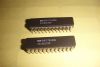
Available in TSSOP package
Pinout Specifications
| Symbol |
Rating |
Max. |
Unit |
| VDD, VDDQ, AVDD |
Supply Voltage Range |
-0.5 to +4.6 |
V |
VI (2)
|
Input Voltage Range |
-0.5 to +5.5 |
V |
VO(2)
|
Voltage Range applied to any
output in the HIGH or LOW state |
-0.5 to
VDD+0.5 |
V |
| IIK (VI < 0) |
Input Clamp Current |
-50 |
mA |
IOK
(VO < 0 or VO > VDD) |
Output Clamp Current |
±50 |
mA |
IO
(VO = 0 to VDD)
|
Continuous Output Current |
±50 |
mA |
| VDD or GND |
Continuous Current |
±200 |
mA |
| TSTG |
Storage Temperature Range |
-65 to +150 |
|
JT
|
Junction Temperature |
+150 |
|
DescriptionThe IDT5V2528A is a high performance, low-skew, low-jitter, phase-lock loop (PLL) clock driver. It uses a PLL to precisely align, in both frequency and phase, the feedback (FBOUT) output to the clock (CLK) input signal.The IDT5V2528 inputs, PLL core, Y0, Y1, and FB
OUT buffers operate from the 3.3V V
DD and AVDD power supply pins.
One bank of ten outputs of the IDT5V2528A provide low-skew, low-jitter copies of CLK. Of the ten outputs, up to seven may be configured for 2.5V or 3.3V LVTTL outputs. The number of 2.5V outputs is controlled by 3-level input signals G_Ctrl and T_Ctrl, and by connecting the appropriate VDDQ pins to 2.5V or
3.3V. The 3-level input signals may be hard-wired to high-mid-low levels. Output signal duty cycles are adjusted to 50 percent, independent of the duty cycle at CLK. The outputs can be enabled or disabled via the G_Ctrl input. When the G_Ctrl input is mid or high, the outputs switch in phase and
frequency with CLK; when the G_Ctrl is low, all outputs (except FB
OUT) are disabled to the logic-low state.
Unlike many products containing PLLs, the IDT5V2528A does not require external RC networks. The loop filter for the PLL is included on-chip, minimizing component count, board space, and cost.
Because it is based on PLL circuitry, the IDT5V2528A requires a stabilization time to achieve phase lock of the feedback signal to the reference signal. This stabilization time is required, following power up and application of a fixed-frequency, fixed-phase signal at CLK, as well as following any changes to the PLL reference or feedback signals. The PLL can be bypassed for test purposes by strapping AV
DD to ground.

 IDT5V2528A Data Sheet