IDT5V9352

Features: • Phase-lock loop clock distribution for high performance clock tree applications• Output enable bank control• External feedback (FBIN) pin is used to synchronize the outputs to the clock input signal• No external RC network required for PLL loop stability• ...

product image

IDT5V9352 Picture
SeekIC No. : 004371898 Detail

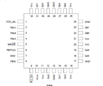
IDT5V9352: Features: • Phase-lock loop clock distribution for high performance clock tree applications• Output enable bank control• External feedback (FBIN) pin is used to synchronize the out...
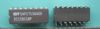
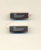
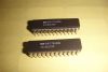
floor Price/Ceiling Price

Part Number:
IDT5V9352
Supply Ability:
5000

Price Break

  • Qty
  • 1~5000
  • Unit Price
  • Negotiable
  • Processing time
  • 15 Days
Total Cost: $ 0.00

SeekIC Buyer Protection PLUS - newly updated for 2013!

  • Escrow Protection.
  • Guaranteed refunds.
  • Secure payments.
  • Learn more >>

Month Sales

268 Transactions

Rating

evaluate  (4.8 stars)

Upload time: 2024/5/3

Payment Methods

All payment methods are secure and covered by SeekIC Buyer Protection PLUS.

Notice: When you place an order, your payment is made to SeekIC and not to your seller. SeekIC only pays the seller after confirming you have received your order. We will also never share your payment details with your seller.
Product Details

Description


Features:

• Phase-lock loop clock distribution for high performance clock tree applications
• Output enable bank control
• External feedback (FBIN) pin is used to synchronize the outputs to the clock input signal
• No external RC network required for PLL loop stability
• Operates at 3.3V/2.5V VCC
• Spread Spectrum Compatible
• Operating frequency up to 200MHz
• Compatible with Motorola MPC9352
• Available in 32-pin TQFP package


Pinout

  Connection Diagram


Specifications

Symbol Description
Max
Unit
VCC Supply Voltage Range
0.5 to +3.6
V
VI Input Voltage
0.5 toVCC +3.6
V
IIN Input Current
±20
V
TSTG Storage Temperature
65 to +150
°C
IOUT DC Output Current
±50
°C
NOTES:
1. Stresses greater than those listed under ABSOLUTE MAXIMUM RATINGS may cause permanent damage to the device. This is a stress rating only and functional operation of the device at these or any other conditions above those indicated in the operational sections of this specification is not implied. Exposure to absolute maximum rating conditions for extended periods may affect reliability.


Description

The IDT5V9352 features three banks of individually configurable outputs. The banks are configured with five, four, and two outputs. The internal divide circuitry allows for output frequency ratios of 1:1, 2:1, 3:1, and 3:2:1. The output frequency relationship is controlled by the fSEL frequency control pins. The fSEL pins, as well as other inputs, are LVCMOS/LVTTL compatible inputs

Unlike many products containing PLLs, the IDT5V9352 does not require external RC networks. The loop filter for the PLL is included on-chip, minimizing component count, board space, and cost.

Because it is based on PLL circuitry, the IDT5V9352 requires a stabilization time to achieve phase lock of the feedback signal to the reference signal. This stabilization time is required, following power up and application of a fixed-frequency, fixed-phase signal at REFCLK, as well as following any changes to the PLL reference or feedback signals. The PLL can be bypassed for test purposes by setting the PLL_EN to high. The 5V9352 is available in Industrial temperature range (-40°C to +85°C).


Customers Who Bought This Item Also Bought

Margin,quality,low-cost products with low minimum orders. Secure your online payments with SeekIC Buyer Protection.
Inductors, Coils, Chokes
Cable Assemblies
Memory Cards, Modules
Batteries, Chargers, Holders
Power Supplies - Board Mount
RF and RFID
View more