Features: • Three internal PLLs• Internal non-volatile EEPROM• JTAG and FAST mode I2C serial interfaces• Input Frequency Ranges: 1MHz to 400MHz• Output Frequency Ranges:− LVTTL: up to 200MHz− LVPECL/ LVDS: up to 500MHz• Reference Crystal Input with p...
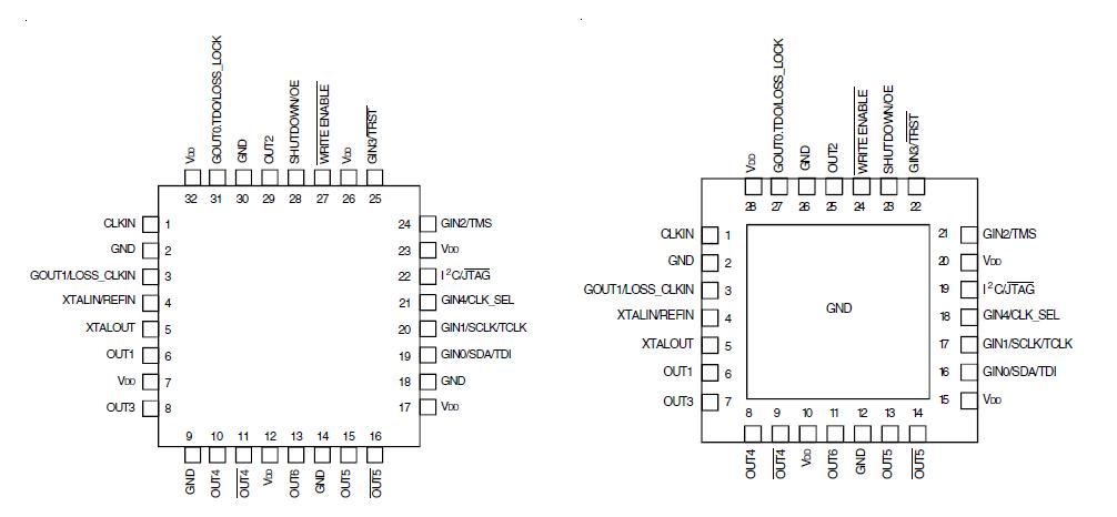
IDT5V9888: Features: • Three internal PLLs• Internal non-volatile EEPROM• JTAG and FAST mode I2C serial interfaces• Input Frequency Ranges: 1MHz to 400MHz• Output Frequency Ranges...
SeekIC Buyer Protection PLUS - newly updated for 2013!
268 Transactions
All payment methods are secure and covered by SeekIC Buyer Protection PLUS.
Features: • IDT54/74FCT646 equivalent to FAST™speed;• IDT54/74FCT646A 30% faster...

|
Symbol |
Description |
Max |
Unit |
|
VDD VI VO TJ TSTG |
Internal Power Supply Voltage Input Voltage Output Voltage(2) Junction Temperature Storage Temperature |
-0.5 to +4.6 |
V V V °C °C |
NOTE:
1. Stresses greater than those listed under ABSOLUTE MAXIMUM RATINGS may cause permanent damage to the device. This is a stress rating only and functional operation of the device at these or any other conditions above those indicated in the operational sections of this specification is not implied. Exposure to absolute maximum rating conditions for extended periods may affect reliability.
2. Not to exceed 4.6V.
The IDT5V9888 is a programmable clock generator intended for high performance data-communications, telecommunications, consumer, and networking applications. There are three internal PLLs, each individually programmable, allowing for three unique non-integer-related frequencies.
The frequencies are generated from a single reference clock. The reference clock can come from one of the two redundant clock inputs. A glitchless automatic or manual switchover function allows any one of the redundant clocks to be selected during normal operation.
The IDT5V9888 can be programmed through the use of the I2C or JTAG interfaces. The programming interface enables the device to be programmed when it is in normal operation or what is commonly known as insystem programmable. An internal EEPROM allows the user to save and restore the configuration of the device without having to reprogram it on power-up. JTAG boundary scan is also implemented.
Each of the three PLLs has an 8-bit pre-scaler and a 12-bit feedback divider. This allows the user to generate three unique non-integer-related frequencies. The PLL loop bandwidth is programmable to allow the user to tailor the PLL response to the application. For instance, the user can tune the PLL parameters to minimize jitter generation or to maximize jitter attenuation. Spread spectrum generation and fractional divides are allowed on two of the PLLs.
There are 10-bit post dividers on five of the six output banks. Two of the six output banks are configurable to be LVTTL, LVPECL, or LVDS. The other four output banks are LVTTL. The outputs are connected to the PLLs via the switch matrix. The switch matrix allows the user to route the PLL outputs to any output bank. This feature can be used to simplify and optimize the board layout. In addition, each output's slew rate and enable/disable function can be programmed.