Features: • 1 to 10 differential clock distribution
• Optimized for clock distribution in DDR2 (Double Data Rate) SDRAM applications
• Operating frequency: 125MHz to 340MHz
• Very low skew: 40ps
• Very low jitter: 40ps
• 1.8V AVDD and 1.8V VDDQ
• CMOS control signal input
• Test mode enables buffers while disabling PLL
• Low current power-down mode
• Tolerant of Spread Spectrum input clock
• Available in 52-Ball VFBGA and 40-pin MLF packagesApplication• Meets or exceeds JEDEC standard 82.8 for registered DDR2 clock driver
• Along with SSTU32864/65/66, DDR2 register, provides complete solution for DDR2 DIMMsPinout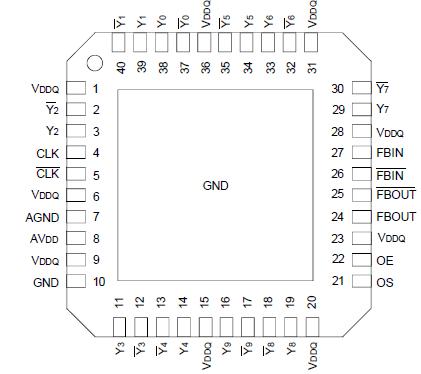 Specifications
| Symbol |
Rating |
Max |
Unit |
| VDDQ, AVDD |
Supply Voltage Range |
0.5 to +2.5 |
V |
| VI(3) |
Input Voltage Range |
0.5 to VDDQ + 0.5 |
V |
| VO(3) |
Voltage range applied to any output in the high or low state |
0.5 to VDDQ + 0.5 |
V |
IIK
(VI <0) |
Input clamp current |
±50 |
mA |
IOK
(VO <0 or
VO > VDDQ) |
Output Clamp Current |
±50 |
mA |
IO
(VO =0 to VDDQ) |
Continuous Output Current |
±50 |
mA |
| VDDQ or GND |
Continuous Current |
±100 |
mA |
| TSTG |
Storage Temperature Range |
65 to +150 |
|
NOTES:
1. Stresses greater than those listed under ABSOLUTE MAXIMUM RATINGS may cause permanent damage to the device. This is a stress rating only and functional operation of the device at these or any other conditions above those indicated in the operational sections of this specification is not implied. Exposure to absolute maximum rating conditions for extended periods may affect reliability.
2. The maximum package power dissipation is calculated using a junction temperature of 150°C and a board trace length of 750 mils.
3. The input and output negative-voltage ratings may be exceeded if the input and output clamp-current ratings are observed. This value is limited to 2.5V max.DescriptionThe CSPU877D is a PLL based clock driver that acts as a zero delay buffer to distribute one differential clock input pair(CLK, CLK ) to 10 differential output pairs (Y [0:9] , Y [0:9]) and one differential pair of feedback clock output (FBOUT, FBOUT). External feedback pins IDTCSPU877D (FBIN, FBIN) for synchronization of the outputs to the input reference is provided. OE, OS, and AVDD control the power-down and test mode logic. When AVDD is grounded, the PLL is turned off and bypassed for test mode purposes. When the differential clock inputs (CLK, CLK) are both at logic low, IDTCSPU877D will enter a low power-down mode. In this mode of IDTCSPU877D, the receivers are disabled, the PLL is turned off, and the output clock drivers are disabled, resulting in a current consumption device of less than 500A.
The CSPU877D requires no external components and has been optimised for very low phase error, skew, and jitter, while maintaining frequency and duty cycle over the operating voltage and temperature range. The CSPU877D, designed for use in both module assemblies and system motherboard based solutions, provides an optimum high-performance clock source.
The CSPU877D is available in Commercial Temperature Range (0°C to +70°C). See Ordering Information for details.

 IDTCSPU877D Data Sheet


