K4D28163HD

Features: • 3.3V + 5% power supply for device operation• 2.5V + 5% power supply for I/O interface• SSTL_2 compatible inputs/outputs• 4 banks operation• MRS cycle with address key programs-. Read latency 3 (clock)-. Burst length (2, 4 and 8)-. Burst type (sequential &a...

product image

K4D28163HD Picture
SeekIC No. : 004382690 Detail

K4D28163HD: Features: • 3.3V + 5% power supply for device operation• 2.5V + 5% power supply for I/O interface• SSTL_2 compatible inputs/outputs• 4 banks operation• MRS cycle with a...

floor Price/Ceiling Price

Part Number:
K4D28163HD
Supply Ability:
5000

Price Break

  • Qty
  • 1~5000
  • Unit Price
  • Negotiable
  • Processing time
  • 15 Days
Total Cost: $ 0.00

SeekIC Buyer Protection PLUS - newly updated for 2013!

  • Escrow Protection.
  • Guaranteed refunds.
  • Secure payments.
  • Learn more >>

Month Sales

268 Transactions

Rating

evaluate  (4.8 stars)

Upload time: 2024/3/28

Payment Methods

All payment methods are secure and covered by SeekIC Buyer Protection PLUS.

Notice: When you place an order, your payment is made to SeekIC and not to your seller. SeekIC only pays the seller after confirming you have received your order. We will also never share your payment details with your seller.
Product Details

Description


Features:

• 3.3V + 5% power supply for device operation
• 2.5V + 5% power supply for I/O interface
• SSTL_2 compatible inputs/outputs
• 4 banks operation
• MRS cycle with address key programs
-. Read latency 3 (clock)
-. Burst length (2, 4 and 8)
-. Burst type (sequential & interleave)
• All inputs except data & DM are sampled at the positive going edge of the system clock
• Differential clock input
• No Wrtie-Interrupted by Read Function
• 2 DQS's ( 1DQS / Byte )
• Data I/O transactions on both edges of Data strobe
• DLL aligns DQ and DQS transitions with Clock transition
• Edge aligned data & data strobe output
• Center aligned data & data strobe input
• DM for write masking only
• Auto & Self refresh
• 32ms refresh period (4K cycle) for -36/-40
• 64ms refresh period (4K cycle) for -50/-60
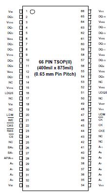
• 66pin TSOP-II
• Maximum clock frequency up to 275MHz
• Maximum data rate up to 550Mbps/pin


Pinout

  Connection Diagram


Specifications

Symbol Symbol Value Unit
Voltage on any pin relative to Vss VIN, VOUT -0.5 ~ 3.6 V
Voltage on VDD supply relative to Vss VDD -1.0 ~ 3.6 V
Voltage on VDD supply relative to Vss VDDQ -0.5 ~ 3.6 V
Storage temperature TSTG -55 ~ +150 °C
Power dissipation PD 1.0 W
Short circuit current IOS 50 mA
Note :Permanent device damage may occur if ABSOLUTE MAXIMUM RATINGS are exceeded.
          Functional operation should be restricted to recommended operating condition.
          Exposure to higher than recommended voltage for extended periods of time could affect device reliability.


Description

The K4D28163HD is 134,217,728 bits of hyper synchronous data rate Dynamic RAM organized as 4 x 2.097,152 words
by 16 bits, fabricated with SAMSUNG 's high performance CMOS technology. Synchronous features with Data Strobe allow extremely high performance up to 1.1GB/s/chip. I/O transactions are possible on both edges of the clock cycle. Range of operating frequencies, programmable burst length and programmable latencies allow the device to be useful for a variety f high performance memory system applications.


Customers Who Bought This Item Also Bought

Margin,quality,low-cost products with low minimum orders. Secure your online payments with SeekIC Buyer Protection.
Test Equipment
Integrated Circuits (ICs)
Cable Assemblies
Power Supplies - Board Mount
View more