K9F1208Q0A-XXB0

Features: · Voltage Supply- 1.8V device(K9F56XXQ0C) : 1.70~1.95V- 3.3V device(K9F56XXU0C) : 2.7 ~ 3.6 V· Organization- Memory Cell Array- X8 device(K9F5608X0C) : (32M + 1024K)bit x 8 bit- X16 device(K9F5616X0C) : (16M + 512K)bit x 16bit- Data Register- X8 device(K9F5608X0C) : (512 + 16)bit x 8bit-...

product image

K9F1208Q0A-XXB0 Picture
SeekIC No. : 004383363 Detail

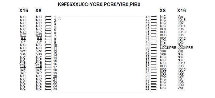
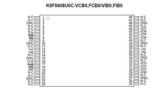
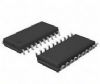
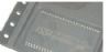
K9F1208Q0A-XXB0: Features: · Voltage Supply- 1.8V device(K9F56XXQ0C) : 1.70~1.95V- 3.3V device(K9F56XXU0C) : 2.7 ~ 3.6 V· Organization- Memory Cell Array- X8 device(K9F5608X0C) : (32M + 1024K)bit x 8 bit- X16 device...

floor Price/Ceiling Price

Part Number:
K9F1208Q0A-XXB0
Supply Ability:
5000

Price Break

  • Qty
  • 1~5000
  • Unit Price
  • Negotiable
  • Processing time
  • 15 Days
Total Cost: $ 0.00

SeekIC Buyer Protection PLUS - newly updated for 2013!

  • Escrow Protection.
  • Guaranteed refunds.
  • Secure payments.
  • Learn more >>

Month Sales

268 Transactions

Rating

evaluate  (4.8 stars)

Upload time: 2024/4/17

Payment Methods

All payment methods are secure and covered by SeekIC Buyer Protection PLUS.

Notice: When you place an order, your payment is made to SeekIC and not to your seller. SeekIC only pays the seller after confirming you have received your order. We will also never share your payment details with your seller.
Product Details

Description


Features:

· Voltage Supply
- 1.8V device(K9F56XXQ0C) : 1.70~1.95V
- 3.3V device(K9F56XXU0C) : 2.7 ~ 3.6 V
· Organization
- Memory Cell Array
- X8 device(K9F5608X0C) : (32M + 1024K)bit x 8 bit
- X16 device(K9F5616X0C) : (16M + 512K)bit x 16bit
- Data Register
- X8 device(K9F5608X0C) : (512 + 16)bit x 8bit
- X16 device(K9F5616X0C) : (256 + 8)bit x16bit
· Automatic Program and Erase
- Page Program
- X8 device(K9F5608X0C) : (512 + 16)Byte
- X16 device(K9F5616X0C) : (256 + 8)Word
- Block Erase :
- X8 device(K9F5608X0C) : (16K + 512)Byte
- X16 device(K9F5616X0C) : ( 8K + 256)Word
· Page Read Operation
- Page Size
- X8 device(K9F5608X0C) : (512 + 16)Byte
- X16 device(K9F5616X0C) : (256 + 8)Word
- Random Access : 10ms(Max.)
- Serial Page Access : 50ns(Min.)
· Fast Write Cycle Time
- Program time : 200ms(Typ.)
- Block Erase Time : 2ms(Typ.)
· Command/Address/Data Multiplexed I/O Port
· Hardware Data Protection
- Program/Erase Lockout During Power Transitions
· Reliable CMOS Floating-Gate Technology
- Endurance : 100K Program/Erase Cycles
- Data Retention : 10 Years
· Command Register Operation
· Intelligent Copy-Back
· Unique ID for Copyright Protection
· Power-On Auto-Read Operation
· Safe Lock Mechanism
· Package
- K9F56XXU0C-YCB0/YIB0
48 - Pin TSOP I (12 x 20 / 0.5 mm pitch)
- K9F56XXX0C-DCB0/DIB0
63- Ball TBGA ( 9 x 11 /0.8mm pitch , Width 1.0 mm)
- K9F5608U0C-VCB0/VIB0
48 - Pin WSOP I (12X17X0.7mm)
- K9F56XXU0C-PCB0/PIB0
48 - Pin TSOP I (12 x 20 / 0.5 mm pitch)- Pb-free Package
- K9F56XXX0C-HCB0/HIB0
63- Ball TBGA ( 9 x 11 /0.8mm pitch , Width 1.0 mm)
- Pb-free Package
- K9F5608U0C-FCB0/FIB0
48 - Pin WSOP I (12X17X0.7mm)- Pb-free Package
* K9F5608U0C-V,F(WSOPI ) is the same device as K9F5608U0C-Y,P(TSOP1) except package type.


Pinout

  Connection Diagram
  Connection Diagram


Specifications

Parameter Symbol Rating Unit
K9F28XXQ0C(1.8V) K9F28XXU0C(3.3V)
Voltage on any pin relative to VSS VIN/OUT -0.6 to + 2.45 -0.6 to + 4.6 V
VCC -0.2 to + 2.45 -0.6 to + 4.6
VCCQ -0.2 to + 2.45 -0.6 to + 4.6
Temperature Under Bias K9F28XXX0C-XCB0 TBIAS -10 to +125
K9F28XXX0C-XIB0 -40 to +125
Storage Temperature K9F28XXX0C-XCB0 TSTG -65 to +150
K9F28XXX0C-XIB0
Short Circuit Current Ios 5 mA
NOTE :
1. Minimum DC voltage is -0.6V on input/output pins. During transitions, this level may undershoot to -2.0V for periods <30ns. Maximum DC voltage on input/output pins is VCC,+0.3V which, during transitions, may overshoot to VCC+2.0V for periods <20ns.
2. Permanent device damage may occur if ABSOLUTE MAXIMUM RATINGS are exceeded. Functional operation should be restricted to the conditions as detailed in the operational sections of this data sheet. Exposure to absolute maximum rating conditions for extended periods may affect reliability.


Description

Offered in 32Mx8bit or 16Mx16bit, the K9F1208Q0A-XXB0 is 256M bit with spare 8M bit capacity. The device is offered in 1.8V or 3.3V Vcc. Its NAND cell provides the most cost-effective solutIon for the solid state mass storage market. A program operation can be performed in typical 200ms on a 528-byte(X8 device) or 264-word(X16 device) page and an erase operation can be performed in typical 2ms on a 16K-byte(X8 device) or 8K-word(X16 device) block. Data in the page can be read out at 50ns cycle time per word. The I/O pins serve as the ports for address and data input/output as well as command input. The on-chip write control automates all program and erase functions including pulse repetition, where required, and internal verification and margining of data. Even the writeintensive systems can take advantage of the K9F1208Q0A-XXB0 s extended reliability of 100K program/erase cycles by providing ECC(Error Correcting Code) with real time mapping-out algorithm.

The K9F1208Q0A-XXB0  is an optimum solution for large nonvolatile storage applications such as solid state file storage and other portable applications requiring non-volatility.


Customers Who Bought This Item Also Bought

Margin,quality,low-cost products with low minimum orders. Secure your online payments with SeekIC Buyer Protection.
Memory Cards, Modules
Isolators
Optical Inspection Equipment
RF and RFID
Potentiometers, Variable Resistors
View more