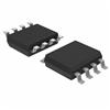
DescriptionThe M25P10AVMN6 is a kind of 1 Mbit, low voltage, serial flash memory. Every instruction sequence starts with a one-byte instruction code. Depending on the instruction, this might be followed by address bytes, or by data bytes, or by both or none. Chip Select (S) must be driven High after the last bit of the instruction se- quence has been shifted in. In the case of a Read Data Bytes (READ), Read Data Bytes at Higher Speed (Fast_Read), Read Identification (RDID), Read Status Register (RD- SR) or Release from Deep Power-down, and Read Electronic Signature (RES) instruction, the shifted-in instruction sequence is followed by a data-out sequence. Chip Select (S) can be driven High after any bit of the data-out sequence M25P10AVMN6 is be- ing shifted out. In the case of a Page Program (PP), Sector Erase (SE), Bulk Erase (BE), Write Status Register (WRSR), Write Enable (WREN), Write Disable (WRDI) or Deep Power-down (DP) instruction, Chip Select (S) must be driven High exactly at a byte boundary, otherwise the instruction is reject- ed, and is not executed. That is, Chip Select (S) must driven High when the number of clock pulses after Chip Select (S) being driven Low is an exact multiple of eight. All attempts to access the memory array during a Write Status Register cycle, Program cycle or Erase cycle are ignored, and the internal Write Status Register cycle, Program cycle or Erase cy- cle continues unaffected. All instructions, addresses and data are shifted in and out of the device, most significant bit first. Serial Data Input (D) is sampled on the first rising edge of Serial Clock (C) after Chip Select (S) is driven Low. Then, the one-byte instruction code must be shifted in to the M25P10AVMN6, most significant bit first, on Serial Data Input (D), each bit being latched on the rising edges of Serial Clock (C). The instruction set is listed in Table 4.
The features of M25P10AVMN6 can be summarized as (1)1 Mbit of flash memory; (2)page program (up to 256 Bytes) in 1.4ms (typical); (3)sector erase (256 Kbit) in 0.8s (typical); (4)bulk erase (1 Mbit) in 2.5s (typical); (5)2.7 to 3.6V single supply voltage; (6)SPI bus compatible serial interface; (7)50MHz clock rate (maximum); (8)deep power-down mode 1A (typical); (9)electronic signature (11h), JEDEC standard two-byte signature (2011h), RES instruction, one-byte, signature (10h), for backward compatibility; (10)more than 100,000 erase/program cycles per sector; (11)more than 20 years' data retention.
The absolute maximum ratings of M25P10AVMN6 are (1)TSTG storage temperature: -65 to 150 °C; (2)TLEAD lead temperature during soldering(1)°C; (3)VIO input and output voltage (with respect to ground): -0.6 to 4.0 V; (4)VCC supply voltage: -0.6 to 4.0 V; (5)VESD electrostatic discharge voltage (human body model):2: -2000 to 2000 V(Note: 1. Compliant with the JEDEC Std J-STD-020C (for small body, Sn-Pb or Pb assembly), the ST ECOPACK 7191395 specification, and the European directive on Restrictions on Hazardous Substances (RoHS) 2002/95/EU. 2. JEDEC Std JESD22-A114A (C1=100 pF, R1=1500, R2=500)).

 M25P10AVMN6 Data Sheet


