Features: SINGLE 2.7 to 3.6V SUPPLY VOLTAGE for PROGRAM, ERASE and READ OPERATIONS
ACCESS TIME: 55ns
PROGRAMMING TIME
10s by Byte typical
11 MEMORY BLOCKS
1 Boot Block (Top or Bottom Location)
2 Parameter and 8 Main Blocks
PROGRAM/ERASE CONTROLLER
Embedded Byte Program algorithm
Embedded Multi-Block/Chip Erase algorithm
Status Register Polling and Toggle Bits
Ready/Busy Output Pin
ERASE SUSPEND and RESUME MODES
Read and Program another Block during Erase Suspend
TEMPORARY BLOCK UNPROTECTION MODE
UNLOCK BYPASS PROGRAM COMMAND
Faster Production/Batch Programming
LOW POWER CONSUMPTION
Standby and Automatic Standby
100,000 PROGRAM/ERASE CYCLES per BLOCK
20 YEARS DATA RETENTION
Defectivity below 1 ppm/year
ELECTRONIC SIGNATURE
Manufacturer Code: 20h
Top Device Code M29W004BT: EAh
Bottom Device Code M29W004BB: EBhPinout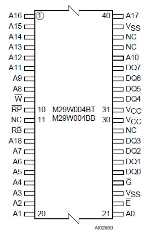 Specifications
|
SYMBOL |
PARAMETER |
Value |
Units |
|
TA |
Ambient Operating Temperature (Temperature Range Option 1) |
0 to 70 |
°C |
|
Ambient Operating Temperature (Temperature Range Option 6) |
40 to 85 |
°C |
|
TBIAS |
Temperature Under Bias |
50 to 125 |
°C |
|
TSTG |
Storage Temperature |
65 to 150 |
°C |
|
VIO(2) |
Input or Output Voltage |
0.6 to 4 |
V |
|
VCC |
Supply Voltage |
0.6 to 4 |
V |
|
VID |
Identification Voltage |
0.6 to 13.5 |
V |
Note: 1. Except for the rating "Operating Temperature Range", stresses above those listed in the Table "Absolute Maximum Ratings" may cause permanent damage to the device. These are stress ratings only and operation of the device at these or any other conditions above those indicated in the Operating sections of this specification is not implied. Exposure to Absolute Maximum Rating conditions for extended periods may affect device reliability. Refer also to the STMicroelectronics SURE Program and other relevant quality documents.
2. Minimum Voltage may undershoot to 2V during transition and for less than 20ns during transitions.DescriptionThe M29W004BB is a 4 Mbit (512Kb x8) non-volatile memory that can be read, erased and reprogrammed. These operations can be performed using a single low voltage (2.7 to 3.6V) supply. On power-up the memory defaults to its Read mode where it can be read in the same way as a ROM or EPROM. The M29W004B is fully backward compatible with the M29W004.
The memory M29W004BB is divided into blocks that can be erased independently so it is possible to preserve valid data while old data is erased. Each block can be protected independently to prevent accidental Program or Erase commands from modifying the memory. Program and Erase commands are written to the Command Interface of the memory. An on-chip Program/Erase Controller simplifies the process of programming or erasing the memory by taking care of all of the special operations that are required to update the memory contents. The end of a program or erase operation can be detected and any error conditions identified. The command set required to control the memory is consistent with JEDEC standards.
The blocks M29W004BB in the memory are asymmetrically arranged, see Tables 3 and 4, Block Addresses. The first or last 64 Kbytes have been divided into four additional blocks. The 16 Kbyte Boot Block can be used for small initialization code to start the microprocessor, the two 8 Kbyte Parameter Blocks can be used for parameter storage and the remaining 32 Kbyte is a small Main Block where the application may be stored.
Chip Enable, Output Enable and Write Enable signals M29W004BB control the bus operation of the memory. They allow simple connection to most microprocessors, often without additional logic.
The memory is offered in a TSOP40 (10 x 20mm) package and it is supplied with all the bits erased (set to '1').

 M29W004BB Data Sheet