MAT02

Features: ·Low Offset Voltage: 50 mV max·Low Noise Voltage at 100 Hz, 1 mA: 1.0 nV/ÖHz max·High Gain (hFE): 500 min at IC = 1 mA 300 min at IC = 1 mA·Excellent Log Conformance: rBE . 0.3 V·Low Offset Voltage Drift: 0.1 mV/8C max·Improved Direct Replacement for LM194/394 Available in Die FormP...

product image

MAT02 Picture
SeekIC No. : 004408331 Detail

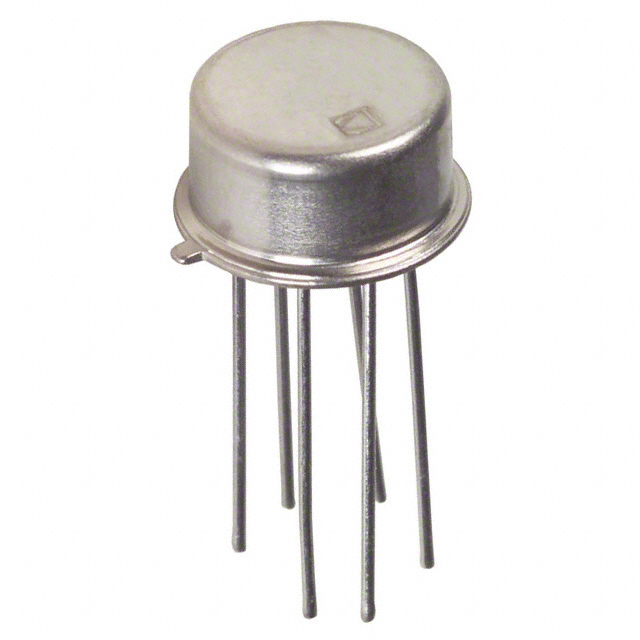
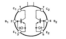
MAT02: Features: ·Low Offset Voltage: 50 mV max·Low Noise Voltage at 100 Hz, 1 mA: 1.0 nV/ÖHz max·High Gain (hFE): 500 min at IC = 1 mA 300 min at IC = 1 mA·Excellent Log Conformance: rBE . 0.3 V·Low ...

floor Price/Ceiling Price

Part Number:
MAT02
Supply Ability:
5000

Price Break

  • Qty
  • 1~5000
  • Unit Price
  • Negotiable
  • Processing time
  • 15 Days
Total Cost: $ 0.00

SeekIC Buyer Protection PLUS - newly updated for 2013!

  • Escrow Protection.
  • Guaranteed refunds.
  • Secure payments.
  • Learn more >>

Month Sales

268 Transactions

Rating

evaluate  (4.8 stars)

Upload time: 2024/4/26

Payment Methods

All payment methods are secure and covered by SeekIC Buyer Protection PLUS.

Notice: When you place an order, your payment is made to SeekIC and not to your seller. SeekIC only pays the seller after confirming you have received your order. We will also never share your payment details with your seller.
Product Details

Description


Features:

·Low Offset Voltage: 50 mV max
·Low Noise Voltage at 100 Hz, 1 mA: 1.0 nV/ÖHz max
·High Gain (hFE): 500 min at IC = 1 mA 300 min at IC = 1 mA
·Excellent Log Conformance: rBE . 0.3 V
·Low Offset Voltage Drift: 0.1 mV/8C max
·Improved Direct Replacement for LM194/394 Available in Die Form


Pinout

  Connection Diagram


Specifications

Collector-Base Voltage (BVCBO) .........................................................40 V Collector-Emitter Voltage (BVCEO) ......................................................40 V Collector-Collector Voltage (BVCC) ......................................................40 V Emitter-Emitter Voltage (BVEE) ....................................................... ....40 V Collector Current (IC) ....................................................................... 20 mA Emitter Current (IE) .......................................................................... 20 mA Total Power Dissipation Case Temperature £ 40°C2 ...............................................................1.8 W Ambient Temperature £ 70°C3 .......................................................500 mW Operating Temperature Range MAT02A ..........................................................................55°C to +125°C MAT02E, F ........................................................................ 25°C to +85°C Operating Junction Temperature ................................... 55°C to +150°C Storage Temperature .................................................... 65°C to +150°C Lead Temperature (Soldering, 60 sec) ............................................ +300°C Junction Temperature..................................................... 65°C to +150°C NOTES 1Absolute maximum ratings apply to both DICE and packaged devices. 2Rating applies to applications using heat sinking to control case temperature. Derate linearly at 16.4 mW/°C for case temperature above 40°C. 3Rating applies to applications not using a heat sinking; devices in free air only. Derate linearly at 6.3 mW/°C for ambient temperature above 70°C.


Description

The design of the MAT02 series of NPN dual monolithic transistors is optimized for very low noise, low drift, and low rBE. Precision Monolithics' exclusive Silicon Nitride "Triple- Passivation" process stabilizes the critical device parameters over wide ranges of temperature and elapsed time. Also, the high current gain (hFE) of the MAT02 is maintained over a wide range of collector current. Exceptional characteristics of the MAT02 include offset voltage of 50 mV max (A/E grades) and 150 mV max F grade. Device performance is specified over the full military temperature range as well as at 25°C.

Input protection diodes are provided across the emitter-base junctions to prevent degradation of the device characteristics due to reverse-biased emitter current. The substrate is clamped to the most negative emitter by the parasitic isolation junction created by the protection diodes. This results in complete isolation between the transistors.

The MAT02 should be used in any application where low noise is a priority. The device can be used as an input stage to make an amplifier with noise voltage of less than 1.0 nV/ÖHz at 100 Hz. Other applications, such as log/antilog circuits, may use the excellent logging conformity of the device. Typical bulk resistance is only 0.3 W to 0.4 W. The MAT02 electrical characteristics approach those of an ideal transistor when operated over a collector current range of 1 mA to 10 mA. For applications requiring multiple devices see MAT04 Quad Matched Transistor data sheet.


Customers Who Bought This Item Also Bought

Margin,quality,low-cost products with low minimum orders. Secure your online payments with SeekIC Buyer Protection.
Batteries, Chargers, Holders
Soldering, Desoldering, Rework Products
Boxes, Enclosures, Racks
Audio Products
Inductors, Coils, Chokes
Connectors, Interconnects
View more