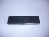
Features: Features of the MC68HC08AZ60A include the following:
•High-Performance M68HC08 Architecture
•Fully Upward-Compatible Object Code with M6805, M146805, and M68HC05 Families
•8.4MHz Internal Bus Frequency at 125°C
•MSCAN08 Controller (Motorola Scalable CAN) (Implementing CAN 2.0b Protocol as Defined in BOSCH Specification Sep. 1991)
•Available in 64 QFP Package
•61,744 Bytes User ROM
•User ROM Data security
•1024 Bytes of On-Chip EEPROM with Security Feature
•2048 Bytes of On-Chip RAM
•Serial Peripheral Interface (SPI) Module
•Serial Communications Interface (SCI) Module
•16-bit Timer Interface Module (TIMA-6) with Six Input Capture/Output Compare Channels
•16-bit Timer Interface Module (TIMB) with Two Input Capture/Output Compare Channels
•Programmable Interrupt Timer (PIT)
•Clock Generator Module (CGM)
•8-Bit, 15-Channel Analog to Digital Convertor (ADC-15)
•5-Bit Keyboard Interrupt Module
•System Protection Features
Computer Operating Properly (COP) with Optional Reset
Low-Voltage Detection with Optional Reset
Illegal Opcode Detection with Optional Reset
Illegal Address Detection with Optional Reset
•Low-Power Design (Fully Static with STOP and WAIT Modes)
•Master Reset Pin and Power-On Reset
Features of the CPU08 include the following:
•Enhanced HC05 Programming Model
•Extensive Loop ControlFunctions
•16 Addressing Modes (8 more than the HC05)
•16-Bit Index Register and Stack Pointer
•Memory-to-Memory Data Transfers
•Fast 8 *8 Multiply Instruction
•Fast 16/8 Divide Instruction
•Binary-Coded Decimal (BCD) Instructions
•Optimization for Controller Applications
•'C' Language Support
Pinout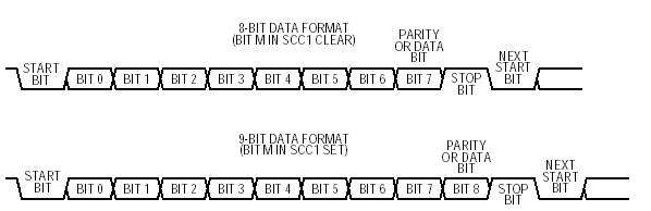 Description
1.4.2 Oscillator Pins MC68HC08AZ48A(OSC1 and OSC2)
The OSC1 and OSC2 pins are the connections for the on-chip oscillator circuit. See Clock Generator Module (CGM) on page 139.
1.4.3 External Reset Pin MC68HC08AZ48A(RST)
A logic '0' on the RST pin forces the MCU to a known start-up state. RST is bidirectional, allowing a reset of the entire system. It is driven low when any internal reset source is asserted. See System Integration Module (SIM) on page 117.
1.4.4 External Interrupt Pin MC68HC08AZ48A(IRQ)
IRQ is an asynchronous external interrupt pin. See External Interrupt Module (IRQ) on page 201.1.4.5 Analog Power Supply Pin (VDDA)VDDA is the power supply pin for the analog portion of the Clock Generator Module (CGM). See Clock Generator Module (CGM) on page 139.
1.4.6 Analog Ground Pin MC68HC08AZ48A(VSSA)V
SSA is the ground connection for the analog portion of the Clock Generator Module (CGM). See Clock Generator Module (CGM) on page 139.
1.4.7 ADC Analog Ground Pin MC68HC08AZ48A(Avss/VREFL)
The AVSS/VREFL pin provides both the analog ground connection and the reference low voltage for the Analog-to-Digital Converter (ADC). See Analog-to-Digital Converter (ADC-15) on page 433.
1.4.8
ADC Reference High Voltage Pin MC68HC08AZ48A(VREFH)
VREFH provides the reference high voltage for the Analog-to-Digital Converter (ADC). See Analog-to-Digital Converter (ADC-15) on page 433.
1.4.9 ADC Analog Power Supply Pin MC68HC08AZ48A(VDDAREF)
VDDAREF is the power supply pin for the analog portion of the Analog-to-Digital Converter (ADC). See Analog-to-Digital Converter (ADC-15)on page 433.
1.4.10 External Filter Capacitor Pin (MC68HC08AZ48ACGMXFC)
CGMXFC is an external filter capacitor connection for the Clock Generator Module (CGM). See Clock Generator Module (CGM) on page 139.
1.4.11 Port A Input/Output (I/O) Pins MC68HC08AZ48A(PTA7PTA0)
PTA7PTA0 are general-purpose bidirectional I/O port pins. See I/O Ports on page 315.
1.4.12 Port B I/O Pins MC68HC08AZ48A(PTB7/ATD7PTB0/ATD0)
Port B is an 8-bit special function port that shares all eight pins with the Analog to Digital Convertor (ADC). See Analog-to-Digital Converter (ADC-15) on page 433 and I/O Ports on page 315.
1.4.13 Port C I/O Pins MC68HC08AZ48A(PTC5PTC0)
PTC5PTC3 andPTC1PTC0 are general-purpose bidirectional I/O port pins. PTC2/MCLK is a special function port that shares its pin with the system clock. See I/O Ports on page 315.1.4.14 Port D I/O Pins (PTD7PTD0/ATD8)Port D is an 8-bit special-function port that shares seven of its pins with the Analog-to-Digital Converter Module (ADC-15), one of its pins with the Timer Interface Module A (TIMA-6), and one more of its pins with the Timer Interface Module B (TIMB). See Timer Interface Module A (TIMA) on page 403 , Timer Interface Module B (TIMB) on page 281, Analog-to-Digital Converter (ADC-15) on page 433 and I/O Ports on page 315.
1.4.15 Port E I/O Pins MC68HC08AZ48A(PTE7/SPSCKPTE0/TxD)
Port E is an 8-bit special function port that shares two of its pins with the Timer Interface Module A (TIMA), four of its pins with the Serial Peripheral Interface Module (SPI), and two of its pins with the Serial Communication Interface Module (SCI). See Serial Communications Interface (SCI) on page 209, Serial Peripheral Interface (SPI) on page 249, Timer Interface Module A (TIMA) on page 403 and I/O Ports on page 315.
1.4.16 Port F I/O Pins MC68HC08AZ48A(PTF6PTF0/TACH2)
Port F is a 7-bit special function port that shares its pins with the Timer Interface Module B (TIMB). Six of its pins are shared with the Timer Interface Module A (TIMA-6). See Timer Interface Module A (TIMA) on page 403, Timer Interface Module B (TIMB) on page 281 and I/O Ports on page 315.
1.4.17 Port G I/O Pins MC68HC08AZ48A(PTG2/KBD2PTG0/KBD0)
Port G is a 3-bit special function port that shares all of its pins with the Keyboard Module (KBD). See Keyboard Module (KBD) on page 395 and I/O Ports on page 315.
1.4.18 Port H I/O Pins MC68HC08AZ48A(PTH1/KBD4PTH0/KBD3)
Port H is a 2-bit special-function port that shares all of its pins with the Keyboard Module (KBD). See Keyboard Module (KBD) on page 395 and I/O Ports on page 315.
1.4.19 CAN Transmit Pin MC68HC08AZ48A (TxCAN)
TxCAN is the digital output from the MSCAN08 module. See MSCAN08 Controller (MSCAN08) on page 343.
1.4.20 CAN Receive Pin MC68HC08AZ48A(RxCAN)
RxCAN is the digital input to the MSCAN08 module. See MSCAN08 Controller (MSCAN08) on page 343.

 MC68HC08AZ48A Data Sheet