Features: `Complete Level 2 Implementation of SS7.
`Compatible with 1988 CCITT, AT&T, ANSI, and Bellcore Signalling System Number 7 link level protocols.
`Optional operation to comply with Japanese TTC JT-Q703 specification requirements
`Pin-for-pin and architecturally compatible with MK50H25 (X.25/LAPD), MK50H29 (SDLC), and MK50H28(FrameRelay).
`System clock rates up to 33 MHz (MK50H27 - 33), or 25 MHz (MK50H27 - 25).
`Data rate up to 4 Mbps continuous for SS7 protocol processing, 20 Mbps for transparent HDLC mode, or up to 51 Mbps bursted (gapped data clocks, non-continuous data).
`On chip DMA control with programmable burst length.
`DMA transfer rate of up to 13.3 Mbytes/sec using optional 5 SYSCLK DMA cycle (150 nS) at 33 MHzSYSCLK.
`Buffer Management includes: - Initialization Block - SeparateReceive and Transmit Rings - Variable Descriptor Ring and Window Sizes.
`Selectable BEC or PCR retransmission methods, including forced retransmission for PCR.
`Handles all 7 SS7 Timers, plus the additional
Signal Unit interval timers for Japanese SS7.
`Handles all SS7 frame formatting: - Zero bit insert and delete - FCS generation and detection - Frame delimiting with flags
`Programmable minimum Signal Unit spacing (number of flags between SU's)
`Handles all sequencing and link control.
`Selectable FCS of 16 or 32 bits.
`Testing Facilities: - InternalLoopback - Silent Loopback - Optional Internal Data Clock Generation - Self Test.
`Programmable for full or half duplex operation
`Programmable Watchdog Timers for RCLK and TCLK (to detect absence of data clocks)
`Available in 52 pin PLCC, 84 pin PLCC(for use with external ROM), or 48 pin DIP packages.
Pinout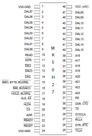 Specifications
|
Symbol |
Parameter |
Value |
Unit |
|
TUB |
Temperature Under Bias |
-25 to +100 |
|
|
TSTG |
Storage Temperature |
-65 to +150 |
|
|
VG |
Voltage on any pin with respect to ground |
-0.5 to VCC+0.5 |
V |
|
PTOT |
Power Dissipation |
0.5 |
W |
Stresses above those listed under "Absolute Maximum Rating" may cause permanent damage to the above device. This is a stress rating only and functional operation of the device at these or any other condition above those ndicated in the operational sections of this specification is not implied. Exposure to absolute maximum rating conditions for xtended periods may affect device reliability.DescriptionThe SGS - Thomson SS7 Signalling Link Controller (MK50H27) is a VLSI semiconductor device which provides a complete level 2 data communication control conforming to the CCITT, ANSI, BELLCORE, and AT&T versions of SS7, as well as options to allow conformance to TTC JT-Q703 (Japanese SS7). This includes signal unit formatting, transparency (so-called "bit-stuffing"), error recovery by two types of retransmission, error monitoring, sequence number control, link status control, and fill in signal unit generation.
One of the outstanding features of the MK50H27 is its buffer management which includes on-chip DMA. This feature allows users to handle multiple MSU's of receive and transmit data at a time. (A conventional data link control chip plus a separate DMA chip would handle data for only a single block at a time.) The MK50H27 will move multiple blocks of receive and transmit data directly into and out of memory through the Host's bus. A possible system configuration for the MK50H27 is shown in figure 1.
For added flexibility a transparent mode provides an HDLC transport mechanism without link layer support. In this mode no protocol processing is done, all data received between opening flag and CRC is written to the shared memory buffer and it is up to the user to take care of the upper level software.
The MK50H27 may be used with any of several popular microprocessors, such as: 68040 ... 68000, 6800, Z8000, Z80, 80486 ... 8086, i960, etc.
The MK50H27 may be operated in either full or half duplex mode. In half duplex mode, the RTS and CTS modem control pins are provided. In full duplex mode, these pins become user programmable I/O pins. All signal pins on the MK50H27 are TTL compatible. This has the advantage of making the MK50H27 independent of the physical interface. As shown in figure 1, line drivers and receivers are used for electrical connection to the physical layer.

 MK50H27 Data Sheet


