MMFTN3018W

DescriptionThe MMFTN3018W is a kind of silicon N-channel MOSFET which can applied in interfacing, switching. The absolute maximum ratings of MMFTN3018W are (1)drain source voltage VDSS: 30 V; (2)gate source voltage VGSS: ± 20 V; (3)drain current ID: 100 mA; (4)drain current (pulsed) IDP 1): 400 m...

product image

MMFTN3018W Picture
SeekIC No. : 004423821 Detail

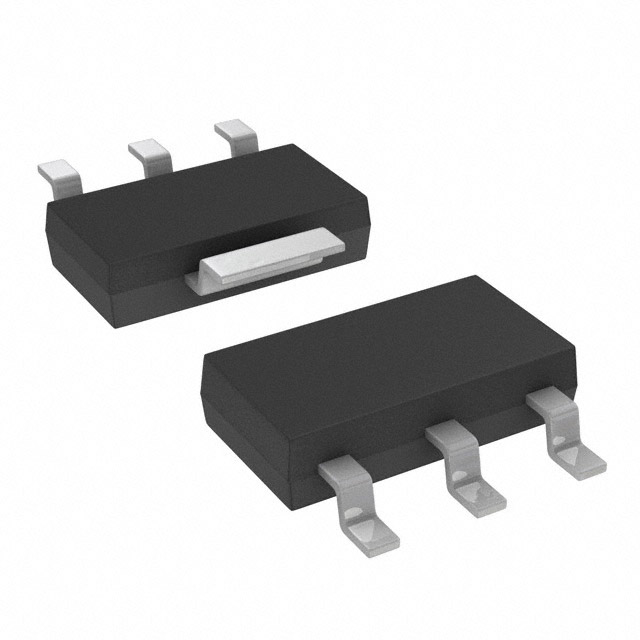
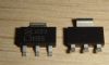
MMFTN3018W: DescriptionThe MMFTN3018W is a kind of silicon N-channel MOSFET which can applied in interfacing, switching. The absolute maximum ratings of MMFTN3018W are (1)drain source voltage VDSS: 30 V; (2)ga...

floor Price/Ceiling Price

Part Number:
MMFTN3018W
Supply Ability:
5000

Price Break

  • Qty
  • 1~5000
  • Unit Price
  • Negotiable
  • Processing time
  • 15 Days
Total Cost: $ 0.00

SeekIC Buyer Protection PLUS - newly updated for 2013!

  • Escrow Protection.
  • Guaranteed refunds.
  • Secure payments.
  • Learn more >>

Month Sales

268 Transactions

Rating

evaluate  (4.8 stars)

Upload time: 2024/6/15

Payment Methods

All payment methods are secure and covered by SeekIC Buyer Protection PLUS.

Notice: When you place an order, your payment is made to SeekIC and not to your seller. SeekIC only pays the seller after confirming you have received your order. We will also never share your payment details with your seller.
Product Details

Description


Description

The MMFTN3018W is a kind of silicon N-channel MOSFET which can applied in interfacing, switching.

The absolute maximum ratings of MMFTN3018W are (1)drain source voltage VDSS: 30 V; (2)gate source voltage VGSS: ± 20 V; (3)drain current ID: 100 mA; (4)drain current (pulsed) IDP 1): 400 mA; (5)total power dissipation Ptot 2): 200 mW; (6)channel temperature Tch: 150°C; (7)storage temperature range Ts: - 55 to + 150°C.

The characteristics at Ta = 25°C of MMFTN3018W can be summarized as (1)drain source breakdown voltage at I D = 10 A V (BR)DSS 30: V; (2)zero gate voltage drain current at V DS = 30 V I DSS : 1 A; (3)gate source leakage current at V GS = ± 20 V ±I GSS : 1 A; (4)gate source threshold voltage at V DS = 3 V, I D = 100 A V GS(th) 0.8: 1.5 V; (5)static drain source on-state resistance at V GS = 4 V, I D = 10 mA R DS(on): 8; (6)static drain source on-state resistance at V GS = 2.5 V, I D = 1 mA R DS(on): 3; (7)forward transfer admittance at V DS = 3 V, I D = 10 mA |y fs | 20: mS; (8)input capacitance at V DS = 5 V, f = 1 MHz C iss: 13pF; (9)output capacitance at V DS = 5 V, f = 1 MHz C oss: 9pF; (10)reverse transfer capacitance at V DS = 5 V, f = 1 MHz C rss: 4 pF.


Customers Who Bought This Item Also Bought

Margin,quality,low-cost products with low minimum orders. Secure your online payments with SeekIC Buyer Protection.
Line Protection, Backups
Sensors, Transducers
Motors, Solenoids, Driver Boards/Modules
Integrated Circuits (ICs)
Programmers, Development Systems
Optical Inspection Equipment
View more