Features: • 288Mb
• 400 MHz DDR operation (800 Mb/s/pin data rate)
• Organization
• 16 Meg x 18, 32 Meg x 9 Separate I/O
• 8 banks
• Cyclic bank switching for maximum bandwidth
• Reduced cycle time (20ns at 400 MHz)
• Nonmultiplexed addresses (address multiplexing option available)
• SRAM-type interface
• Read latency (RL), row cycle time, and burst sequence length
• Balanced READ and WRITE latencies in order to optimize data bus utilization
• Data mask for WRITE commands
• Differential input clocks (CK, CK#)
• Differential input data clocks (DKx, DKx#)
• On-chip DLL generates CK edge-aligned data and output data clock signals
• Data valid signal (QVLD)
• 32ms refresh (8K refresh for each bank; 64k refresh command must be issued in total each 32ms)
• 144-ball FBGA package
• HSTL I/O (1.5V or 1.8V nominal)
• 2560 matched impedance outputs
• 2.5V VEXT, 1.8V VDD, 1.5V or 1.8V VDDQ I/O
• On-die termination (ODT) RTT
Pinout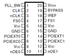 Specifications
Storage Temperature . . . . . . . . . . . . . . . . . . . . . . . .-55°C to +150°C
I/O Voltage . . . . . . . . . . . . . . . . . . . . . . . . . . . . -0.3V to VDDQ + 0.3V
Voltage on VEXT Supply Relative to VSS . . . . . . . . . . . -0.3V to +2.8V
Voltage on VDD Supply Relative to VSS . . . . . . . . . . . . -0.3V to +2.1V
Voltage on VDDQ Supply Relative to VSS . . . . . . . . . . . -0.3V to +2.1V
Junction Temperature** . . . . . . . . . . . . . . . . . . . . . . . .. . . .. . .110°C
DescriptionThe Micron® 288Mb reduced latency DRAM (RLDRAM) II MT49H16M18C is a high-speed memory device designed for high bandwidth communication data storage. Applications include, but are not limited to, transmitting or receiving buffers in telecommunication systems and data or instruction cache applications requiring large amounts of memory. The MT49H16M18C's eightbank architecture is optimized for high speed and achieves a peak bandwidth of 28.8 Gb/s, using two separate 18-bit double data rate (DDR) parts and a maximum system clock of 400 MHz.
The DDR separate I/O interface of MT49H16M18C transfers two 18- or 9-bit wide data word per clock cycle at the I/O balls. The read port has dedicated data outputs to support READ operations, while the write port has dedicated input balls to support WRITE operations. Output data is referenced to the free-running output data clock. This architecture of MT49H16M18C eliminates the need for high speed bus turnaround.
Commands, addresses, and control signals of MT49H16M18C are registered at every positive edge of the differential input clock, while input data is registered at both positive and negative edges of the input data clock(s).
Read and write accesses to the RLDRAM MT49H16M18C are burstoriented. The burst length is programmable from 2, 4, or 8 by setting the mode register.
The MT49H16M18C is supplied with 2.5V and 1.8V for the core and 1.5V or 1.8V for the output drivers.
Bank-scheduled refresh of MT49H16M18C is supported with row address generated internally.
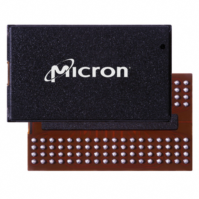
A standard FBGA 144-ball package is used to enable ultra high-speed data transfer rates and a simple upgrade path from former products.

 MT49H16M18C Data Sheet