MX29L8000B

Features: • Extended single-supply voltage range 2.7V to 3.6V for read and write• JEDEC-standard EEPROM commands• Endurance : 100,000 cycles• Fast access time: 120ns• Optimized block architecture- One 16 Kbyte protected block(16K-block)- Two 8 Kbyte parameter blocks- ...

product image

MX29L8000B Picture
SeekIC No. : 004431738 Detail

MX29L8000B: Features: • Extended single-supply voltage range 2.7V to 3.6V for read and write• JEDEC-standard EEPROM commands• Endurance : 100,000 cycles• Fast access time: 120ns• O...

floor Price/Ceiling Price

Part Number:
MX29L8000B
Supply Ability:
5000

Price Break

  • Qty
  • 1~5000
  • Unit Price
  • Negotiable
  • Processing time
  • 15 Days
Total Cost: $ 0.00

SeekIC Buyer Protection PLUS - newly updated for 2013!

  • Escrow Protection.
  • Guaranteed refunds.
  • Secure payments.
  • Learn more >>

Month Sales

268 Transactions

Rating

evaluate  (4.8 stars)

Upload time: 2024/6/7

Payment Methods

All payment methods are secure and covered by SeekIC Buyer Protection PLUS.

Notice: When you place an order, your payment is made to SeekIC and not to your seller. SeekIC only pays the seller after confirming you have received your order. We will also never share your payment details with your seller.
Product Details

Description


Features:

• Extended single-supply voltage range 2.7V to 3.6V for read and write
• JEDEC-standard EEPROM commands
• Endurance : 100,000 cycles
• Fast access time: 120ns
• Optimized block architecture
- One 16 Kbyte protected block(16K-block)
- Two 8 Kbyte parameter blocks
- One 96 Kbyte main block
- Seven 128 Kbyte main blocks
• Hardware and software data protection
- Hardware Write Protection pin (WP)
- Hardware Lockout bit for 16K-block
- Software command data protection
• Software EEPROM emulation with parameter blocks
• Status register
- For detection of program or erase cycle completion
• Auto Erase operation
- Automatically erases any one of the sectors or the whole chip
- Erase suspend capability
- Fast erase time: 50ms typical for chip erase
• Auto Page Program operation
- Automatically programs and verifies data at specified addresses
- Internal address and data latches for 128 bytes per page
• Low power dissipation
- 20mA active current
- 20uA standby current
- 1uA deep power-down current
• Hardware Reset pin (RP)
- Reset internal state machine, and put the device into deep power-down mode
• Built-in 128 Bytes Page Buffer
- Work as SRAM for temporary data storage
- Fast access to temporary data
• Low Vcc write inhibit 1.8V
• Industry standard surface mount packaging
- 40-Lead TSOP Type I


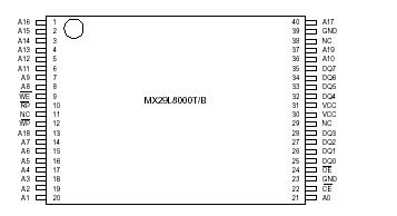
Pinout

  Connection Diagram


Specifications

RATING

VALUE

Ambient Temperature -40°C to 85°C
Storage Temperature

-65°C to 125°C

Applied Input Voltage

-0.5V to VCC + 4.5

Applied Output Voltage -0.5V to VCC + 0.6
VCC to Ground Potential -0.5V to 5.5V
A9,WP

-0.5V to 13.0V


Description

The MX29L8000T/MX29L8000B is a 8 Mbit, 3 V-only Flash memory organized as a 1 Mbytes of 8 bits each. For flexible erase and program capability, the 8 Mbits of data is divided into 11 sectors of one 16 Kbyte protected block, two 8 Kbyte parameter blocks, one 96 Kbyte main block, and seven 128 Kbyte main blocks. To allow for simple in-system operation, the device can be operated with a single 2.7 V to 3.6 V supply voltage. Since many designs read from the flash memory a large percentage of the time,significant power saving is achieved with the 2.7 V VCC operation. Manufactured with MXIC's advanced nonvolatile memory technology, the device offers access times of 120 ns, and a low 1uA typical deep power-down current.

The MX29L8000T/MX29L8000B command set is compatible with the JEDEC single-power-supply flash standard. Commands are written to the command register using standard microprocessor write timings. MXIC's flash memory augments EPROM functionality with an internal state machine which controls the erase and program circuitry.The device Status Register provides a convenient way to monitor when a program or erase cycle is complete, and the success or failure of that cycle.

Programming the MX29L8000T/MX29L8000B is performed on a page basis; 128 bytes of data are loaded into the device and then programmed simultaneously. The typical Page Program time is 5ms.The device can also be reprogrammed in standard EPROM programmers.Reading data out of the device is similar to reading from an EPROM or other flash.

Erase is accomplished by executing the Erase command sequence. This will invoke the Auto Erase algorithm which is an internal algorithm that automatically times the erase pulse widths and verifies proper cell margin. This device features both chip erase and block erase. Each block can be erased and programmed without affecting other blocks. Using MXIC's advanced design technology, no preprogram is required (internally or externally). As a result, the whole MX29L8000B can be typically erased and verified in as fast as 50 ms.

A combined feature of Write Protection pin (WP), Reset pin (RP), 16K-block lockout bit, and software command sequences provides complete data protection. First,software data protection protects the device from inadvertent program or erase. Two "unlock" write cycles must be presented to the device before the program or erase command can be accepted by the device. For hardware data protection, the WP pin and RP pin provide protection against unwanted command writes due to invalid system bus condition that may occur during system reset and power-up/down sequence. Finally, with 16K-block lockout bit feature, the MX29L8000B provides complete core security for the kernel code required for system initialization.


Customers Who Bought This Item Also Bought

Margin,quality,low-cost products with low minimum orders. Secure your online payments with SeekIC Buyer Protection.
Integrated Circuits (ICs)
Line Protection, Backups
Batteries, Chargers, Holders
Potentiometers, Variable Resistors
Prototyping Products
DE1
Optical Inspection Equipment
View more