Features: GENERAL FEATURES
• Single Power Supply Operation
- 2.7 to 3.6 volt for read, erase, and program operations
• 8,388,608 x 8 / 4,194,304 x 16 switchable
• Sector structure
- 8KB (4KW) x 8 and 64KB(32KW) x 127
• Sector Protection/Chip Unprotect
- Provides sector group protect function to prevent program or erase operation in the protected sector group
- Provides chip unprotect function to allow code changes
- Provides temporary sector group unprotect function for code changes in previously protected sector groups
• Secured Silicon Sector
- Provides a 128-word area for code or data that can be permanently protected.
- Once this sector is protected, it is prohibited to program or erase within the sector again.
• Latch-up protected to 250mA from -1V to Vcc + 1V
• Low Vcc write inhibit is equal to or less than 1.5V
• Compatible with JEDEC standard
- Pin-out and software compatible to single power supply Flash
SOFTWARE FEATURES
• Support Common Flash Interface (CFI)
- Flash device parameters stored on the device and provide the host system to access.
• Erase Suspend/ Erase Resume
- Suspends sector erase operation to read data from or program data to another sector which is not being erased
• Status Reply
- Data polling & Toggle bits provide detection of program and erase operation completion
HARDWARE FEATURES
• Ready/Busy (RY/BY) Output
- Provides a hardware method of detecting program and erase operation completion
• Hardware Reset (RESET) Input
- Provides a hardware method to reset the internal state machine to read mode
• WP Pin
- Write protect (WP) function allows protection of two outermost boot sectors, regardless of sector protect status
Pinout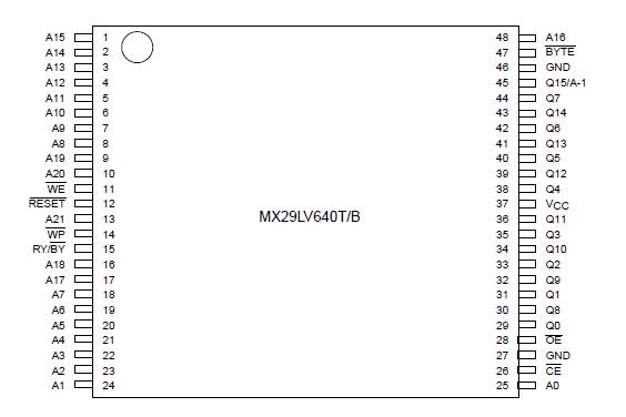 Specifications
Storage Temperature
Plastic Packages ..............-65oC to +150oC
Ambient Temperature
with Power Applied.............-65oC to +125oC
Voltage with Respect to Ground
VCC (Note 1) ............... -0.5 V to +4.0 V
A9, OE, and
RESET (Note 2) .............-0.5 V to +12.5 V
All other pins (Note 1) .......-0.5 V to VCC +0.5 V
Output Short Circuit Current (Note 3) . . . . . . 200 mA
Notes:
1. Minimum DC voltage on input or I/O pins is -0.5 V. During voltage transitions, input or I/O pins may overshoot VSS to -2.0 V for periods of up to 20 ns. See Figure 6. Maximum DC voltage on input or I/O pins is VCC +0.5 V. During voltage transitions, input or I/O pins may overshoot to VCC +2.0 V for periods up to 20 ns. See Figure 7.
2. Minimum DC input voltage on pins A9, OE, and RESET is -0.5 V. During voltage transitions, A9, OE, and RESET may overshoot VSS to -2.0 V for periods of up to 20 ns. See Figure 6. Maximum DC input voltage on pin A9 is +12.5 V which may overshoot to 14.0 V for periods up to 20 ns.
3. No more than one output may be shorted to ground at a time. Duration of the short circuit should not be greater than one second.
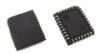
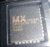
DescriptionThe MX29LV640T/B is a 64-mega bit Flash memory organized as 8M bytes of 8 bits or 4M bytes of 16 bits. MXIC's Flash memories offer the most cost-effective and reliable read/write non-volatile random access memory. The MX29LV640T/B is packaged in 48-pin TSOP, 63- ball CSP and 64-ball Easy BGA. It is designed to be reprogrammed and erased in system or in standard EPROM programmers.
The standard MX29LV640T/B offers access time as fast as 90ns, allowing operation of high-speed microprocessors without wait states. To eliminate bus contention, the MX29LV640T/B has separate chip enable (CE) and output enable (OE) controls.
MXIC's Flash memories augment EPROM functionality with in-circuit electrical erasure and programming. The 2 P/N:PM0920 REV. 1.2, NOV. 05, 2003 MX29LV640T/B MX29LV640T/B uses a command register to manage this functionality.
MXIC Flash technology reliably stores memory contents even after 100,000 erase and program cycles. The MXIC cell is designed to optimize the erase and program mechanisms. In addition, the combination of advanced tunnel oxide processing and low internal electric fields for erase and programming operations produces reliable cycling. The MX29LV640T/B uses a 2.7V to 3.6V VCC supply to perform the High Reliability Erase and auto Program/Erase algorithms.
The highest degree of latch-up protection is achieved with MXIC's proprietary non-epi process. Latch-up protection is proved for stresses up to 100 milliamperes on address and data pin from -1V to VCC + 1V.

 MX29LV640T Data Sheet