Features: • 16A, 60V• rDS(ON) = 0.047Ω• Temperature Compensating PSPICE® Model• Can be Driven Directly from CMOS, NMOS, TTL Circuits• Peak Current vs Pulse Width Curve• UIS Rating Curve• Related Literature - TB334 Guidelines for Soldering Surfac...
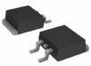
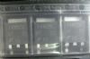
RFD16N06LESM: Features: • 16A, 60V• rDS(ON) = 0.047Ω• Temperature Compensating PSPICE® Model• Can be Driven Directly from CMOS, NMOS, TTL Circuits• Peak Current vs Pulse Wi...
SeekIC Buyer Protection PLUS - newly updated for 2013!
268 Transactions
All payment methods are secure and covered by SeekIC Buyer Protection PLUS.
| RFD16N06LESM | UNITS | |
| Drain to Source Voltage (Note 1) VDSS | 60 | V |
| Drain to Gate Voltage (RGS = 1MW) (Note 1)VDGR | 60 | V |
| Continuous (Figure 2)ID | 16 | A |
| Pulsed Drain Current (Note 3) IDM | Refer to Peak Current Curve | A |
| Gate to Source Voltage VGS | +10, -8 | V |
Pulsed Drain Current IDM |
Refer to UIS Curve |
W |
| Power Dissipation | 90 | |
| Derate above 25oC | 0.606 | A |
| Pulsed Avalanche Rating UIS | Refer to UIS SOA | |
| Operating and Storage Temperature .TJ, TSTG | -55 to 75 | o C |
| Maximum Temperature for Soldering | ||
| Leads at 0.063in (1.6mm) from Case for 10s TL | 300 | o C |
| Package Body for 10s, See Techbrief 334 Tpkg | 260 | o C |
These are N-Channel power MOSFETs RFD16N06LESM manufactured using a modern process. This process, which uses feature sizes approaching those of LSI integrated circuits gives optimum utilization of silicon, resulting in outstanding performance. They were designed for use in applications such as switching regulators, switching converters, motor drivers, relay drivers and emitter switches for bipolar transistors. This performance is accomplished through a special gate oxide design which provides full rated conductance at gate bias in the 3V to 5V range, thereby facilitating true on-off power control directly from logic level (5V) integrated circuits