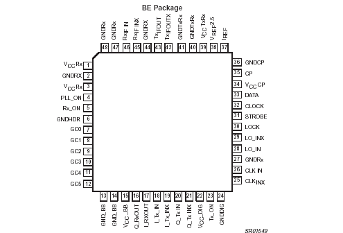
Features: • Low supply voltage operation of 2.7 V for main chip and 2.9 V for charge pump.• Low current consumption: 33.5 mA in RX, 26.5 mA in TX, typical at 3 V.• Flexible power up/down options.• Optional 2.5 V regulated reference voltage available during transmit.• ...
SA1630: Features: • Low supply voltage operation of 2.7 V for main chip and 2.9 V for charge pump.• Low current consumption: 33.5 mA in RX, 26.5 mA in TX, typical at 3 V.• Flexible power u...
SeekIC Buyer Protection PLUS - newly updated for 2013!
268 Transactions
All payment methods are secure and covered by SeekIC Buyer Protection PLUS.

|
SYMBOL |
PARAMETER |
RATING |
UNITS |
|
VCCXX |
Supply voltages |
0.3 to +6.0 |
V |
|
VIN |
Voltage applied to any other pin |
-0.3 to (VCCXX+0.3) |
V |
|
VG |
Any GND pin to any other GND pin |
0 |
V |
|
PD |
Power dissipation, TA = 25 (still air) |
300 |
mW |
|
TJMAX |
Maximum operating junction temperature |
150 |
|
|
PMAX |
Maximum power input/output |
+20 |
dBm |
|
TSTG |
Storage temperature range |
65 to +150 |
The SA1630 is a 70400 MHz I/Q transceiver for wireless LAN. The Receive Path contains a digitally gain controlled linear IF amplifier, a pair of quadrature down conversion mixers and a pair of baseband amplifiers. The SA1630 transmit path contains a pair of quadrature up conversion mixers that transposes a quadrature baseband input signal up to IF frequency. An external VCO signal is divided internally and provides quadrature local oscillator signals for the mixers. Another divider chain of SA1630 , reference divider and phase detector are provided to avoid the need for an external synthesizer. To keep power consumption to a minimum the transmit, receive and local oscillator functions can be powered down under digital control.