Features: 8051 compatible microcontroller with TV related special features and advanced OSD display Feature selection via special function register Simultaneous processing of TTX, VPS, PDC and WSS (line 23) data Supply voltage 2.5 V for core and 3.3 V for ports ROM version package PSDIP52-2, PMQF...
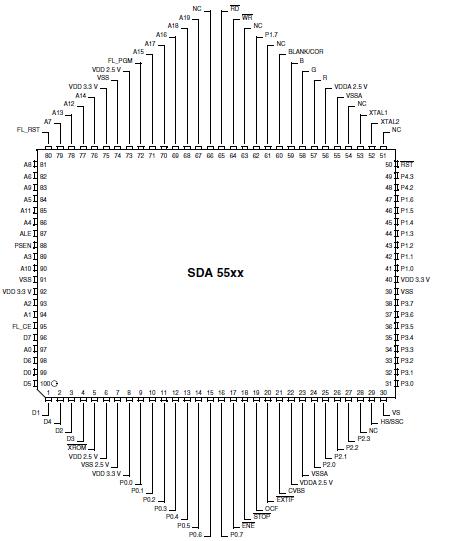
SDA5525: Features: 8051 compatible microcontroller with TV related special features and advanced OSD display Feature selection via special function register Simultaneous processing of TTX, VPS, PDC and WSS ...
SeekIC Buyer Protection PLUS - newly updated for 2013!
268 Transactions
All payment methods are secure and covered by SeekIC Buyer Protection PLUS.

|
Symbol |
Parameter | Pin Name | Pin Name | Unit | |
| Min | Max | ||||
|
TA |
Ambient Temperature PSDIP52-1, PSDIP52-2 1) PMQFP64-1 PLCC84-1 PMQFP100-1 |
−10 −10 −10 −10 |
70 70 70 70 |
°C °C °C °C | |
|
TC |
Case Temperature PSDIP52-1, PSDIP52-2 1 PMQFP64-1 PLCC84-1 PMQFP100-1 |
15 15 15 15 |
85 85 85 85 |
°C °C °C °C | |
|
TS |
Storage Temperature | -20 | 125 | °C | |
|
Pmax |
Maximum Power Dissipation PSDIP52-1, PSDIP52-2 1) PMQFP64-1 PLCC84-1 PMQFP100-1 |
0.6 0.6 0.6 0.6 |
W | ||
| VDD331..7 | Supply Voltage 3.3 V | 3 | 3.6 | V | |
| VDD251..2 | Supply Voltage 2.5 V | 2.25 | 2.75 | - | |
| VDDA1..4 | Analog Supply Voltage | 2.25 | 2.75 | - | |
| 1) Single chip. Not applicable for Flash version (SDA 555xFL) | |||||
The on-chip clock generator SDA5525 provides the TVTpro with its basic clock signal. The oscillator runs with an external crystal and the appropriate internal oscillator circuitry (see Fig. on page 174).
For applications with lower timing accuracy requirements (and if the RTC is not used) an external ceramic resonator SDA5525 can be used. The usage of a ceramic resonator is not recommended for Teletext applications as depending on the absolute tolerance of the ceramic resonator the data slicer may not work correctly. Additional SDA5525 might also require that display timing parameters and the baud rate prescaler have to be adapted.
In timing critical applications the horizontal frequency of the incoming CVBS signal SDA5525 can be used to measure the actual timing deviation and to re-program the clock PLL.
The 6 MHz clock signal SDA5525 is used to generate the internal 300 MHz display reference clock by means of an onchip phase locked loop (PLL). The PLL can be bypassed to reduce the power consumption. If an immediate wake up from power down is not required the PLL can also be switched off in SDA5525. From the output frequency of the main clock PLL two clock systems are derived.