SeekIC No. : 004486887
Detail
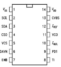
SDA5642X: Features: mC suitable VPS data editing direct from CVBS signaln-channel MOSGenerating of the line synchronous 5-MHz clock for the time base and data clock by means of PLL operationVery few external ...
 SDA5642X Data Sheet
floor Price/Ceiling Price
- Part Number:
- SDA5642X
- Supply Ability:
- 5000
Price Break
- Qty
- 1~5000
- Unit Price
- Negotiable
- Processing time
- 15 Days
SeekIC Buyer Protection PLUS - newly updated for 2013!
- Escrow Protection.
- Guaranteed refunds.
- Secure payments.
- Learn more >>
Month Sales
268 Transactions
Payment Methods
All payment methods are secure and covered by SeekIC Buyer Protection PLUS.
Notice: When you place an order, your payment is made to SeekIC and not to your seller. SeekIC only pays the seller after confirming you have received your order. We will also never share your payment details with your seller.