Features: • Different application modes
- SRC mode:
- High performance scan rate converter
- High performance scan rate converter plus high resolution frame based joint-linefree Picture-in-Picture (maximum approximately 1/9 picture)
- SSC mode:
- Split screen applications with two signal sources (e.g. double window)
- MUP mode:
- Multipicture display mode (e.g. tuner scan)
• 8 bit amplitude resolution of each input channel
- Two input channels
- Input frequency up to 27 MHz
- ITU-R 656 data format (8 wires data only and additional sync information or 8 wires including sync information)
- 4:2:2 luminance and chrominance parallel (2x8 wires)
• Two different representations of input chrominance data
- 2's complement code
- Positive dual code
• Two flexible input sync controllers
• Vertical peaking of the input signal
• Flexible scaling of the input signal
- Flexible digital vertical compression of the input signal (1.0, ... [2 line resolution] ... , 1/32)
- Flexible horizontal compression and expansion of the input signal (2.0, ... [4 pixel resolution] ... ,1.0 , ... [4 pixel resolution] ... , 1/32)
- Panorama mode (programmable characteristic)
• Noise reduction
- Motion adaptive spatial and temporal noise reduction (3D-NR)
- Temporal noise reduction for luminance and chrominance, frame based or field based
- Different motion detectors for luminance and chrominance or identical
- Flexible programming of the temporal noise reduction parameters
- Automatic measurement of the noise level (5 bit value, readable by I²C-bus)
• 3-D motion estimation
- High performance motion estimation based on block matching algorithm
- Film mode detector (PAL and NTSC), Global motion flag (readable by I²C bus)
• Automatic detection of letter box formats (readable by I²C bus)
• TV mode detection by counting line numbers (PAL, NTSC, readable by I²C bus)
• Embedded memory
- 6 Mbit embedded DRAM core for field memories
- 1,1 Mbit embedded DRAM core for line memories, vector memory, block-to-line converter
- 36 kbit SRAM for block matching, line-to-block converter
• Flexible clock and synchronization concept
- Decoupling of the input and output clock system possible
• Scan rate conversion
- Motion compensated 100/120 Hz interlaced scan conversion (Micronas VDU)
- Motion compensated 50/60 Hz progressive scan conversion (Micronas VDU)
- Simple interlaced modes: ABAB, AABB, AAAA, BBBB
- Simple progressive modes: AB, AA*, B*B
- True Motion: 50 Hz motion resolution even for 25 Hz PAL film sources 60 Hz motion resolution even for 30 Hz NTSC film sources
- Large area and line flicker reduction
• Flexible digital vertical expansion of the output signal (1.0, ... [1/64] ... , 2.0)
• Sharpness improvement
- Digital colour transition improvement (DCTI)
- Digital luminance transition improvement (DLTI)
- Peaking (luminance only)
• Flexible output sync controller
- Flexible positioning of the two output channels in all application modes
- Flexible height and width of the two output pictures
- Flexible programming of the output sync raster
• Signal manipulations
- Still frame or field
- Insertion of coloured background
- Insertion of a selection border
- Adjustable delay between Y and UV signal (+4,...[1]...,-3 input pixels) at the input side
- Adjustable delay between Y and UV signal (+3,...[0.5]...,- 4 output pixels) at the output side
• Three D/A converters
- 9 bit amplitude resolution for Y, -(R-Y), -(B-Y) output
- 60 MHz maximal clock frequency
- Two-fold oversampling
- Simplification of external analog post filtering and differential analog outputs
• I²C-bus control (400 kHz)
• P-MQFP-100 package
• 3.3 V ± 5% supply voltage
Pinout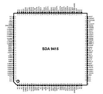 Specifications
| Parameter |
Symbol |
Min |
Max |
Unit |
Remark |
| Operating Temperature |
TA |
0 |
70 |
°C |
|
| Storage Temperature |
Tstg |
-65 |
125 |
°C |
|
| Junction Temperature |
TJ |
|
125 |
°C |
|
| Soldering Temperature |
TS |
|
260 |
°C |
|
| Soldering Time |
tS |
|
10 |
s |
|
| Input Voltage |
VI |
-0.3 |
VDD+0.3 |
V |
not valid for I²C Bus pins |
| Output Voltage |
VQ |
-0.3 |
VDD+0.3 |
V |
not valid for I²C Bus pins |
| Input Voltage |
VI |
-0.3 |
5.5 |
V |
I²C Bus pins only |
| Output Voltage |
VO |
-0.3 |
5.5 |
V |
I²C Bus pins only |
| Supply Voltages |
VDD |
-0.3 |
3.8 |
V |
|
| Supply voltage differentials |
VDD |
-0.25 |
0.25 |
V |
between any internally non-connected
supply pins of the same kind, see Pin
Configuration |
| DAC output current |
IO |
-30 |
|
mA |
for any single output |
| DAC output voltage |
|
-0.3 |
VDD+0.3 |
mA |
for any single output |
| RREF_I output current |
IO |
-5 |
|
mA |
for any single output |
| Total Power Dissipation |
THD |
|
1.8 |
W |
|
| ESD Protection |
ESD |
-2,0 |
2,0 |
kV |
MIL STD 883C method
3015.6, 100pF, 1500(HMB) |
| ESD Protection |
ESD |
-1,5 |
-1,5 |
kV |
EOS/ESD Assn. Standard DS 5.3-1993
(CDM) |
| |
|
|
|
|
|
| Latch-Up Protection |
|
-100 |
100 |
mA |
all inputs/outputs |
DescriptionThe SDA 9415 is the first single-chip Micronas MEGAVISION® feature box including scan rate conversion and the necessary field memories, a second input channel for split screen applications like picture-and-picture and digital-to-analog converters. The SDA 9415 has three application modes: the SRC (Scan Rate Conversion) mode, the SSC
(Split SCreen) mode and the MUP (MUlti Picture) mode.
The two input channels of the SDA 9415 are not equivalent. One input channel is always the so called "master" channel and one input channel is always the so called "slave" channel. Both channels are combined of the output side of the SDA 9415 in the "MUX" block. The master channel of SDA 9415 is always the "synchronization" master of both channels.
In the SRC mode the SDA 9415 can be used as a high performance scan rate converter. Scan rate conversion is done by a motion compensated algorithm known as Micronas VDU (Vector Driven Up conversion). In addition a high resolution frame based joint-linefree
picture-and-picture (maximum approximately 1/9 picture) of SDA 9415 can be displayed. The figure below shows an example of the SRC mode.
For this usage the 6 Mbit eDRAM core is separated in two luminance fields and two chrominance fields (either 4:2:0 or 4:1:1) and a memory area for luminance and chrominance fields (4:1:1) [maximum circa 1/9 picture] for picture-in-picture applications. The vector based scan rate conversion of SDA 9415 is possible for the master channel only.
For the SSC mode the 6 Mbit eDRAM core is split in two 3 Mbit areas, SDA 9415 is able to contain a maximum of two luminance fields and two chrominance fields (either 4:2:0 or 4:1:1). The figure below shows different applications ("Double window", "Zoom-in-zoomout"). In this case only a simple scan rate conversion (e.g. field doubling for interlaced conversion: AABB) for both output channels is possible.
The MUP mode of SDA 9415 allows the combination of one life picture and a configuration of still pictures. The figure below shows an application. In this case only a simple scan rate conversion (e.g. field doubling for interlaced conversion: AABB or AAAA) is possible.
The behaviour of the master and the slave channel of SDA 9415 does not differ in general. Therefore for further description of the master and the slave channel the figures are also valid for both unless it is pointed out.

 SDA9415 Data Sheet