Features: • Three-step gain control, cellular LNA• External resistor to adjust LNA bias current• Buffered LO signal for transmit upconverter• VGA with 90 dB dynamic range• Integrated IF VCO and tank circuit• VCO_ON auto-tuning control• Battery cell operati...
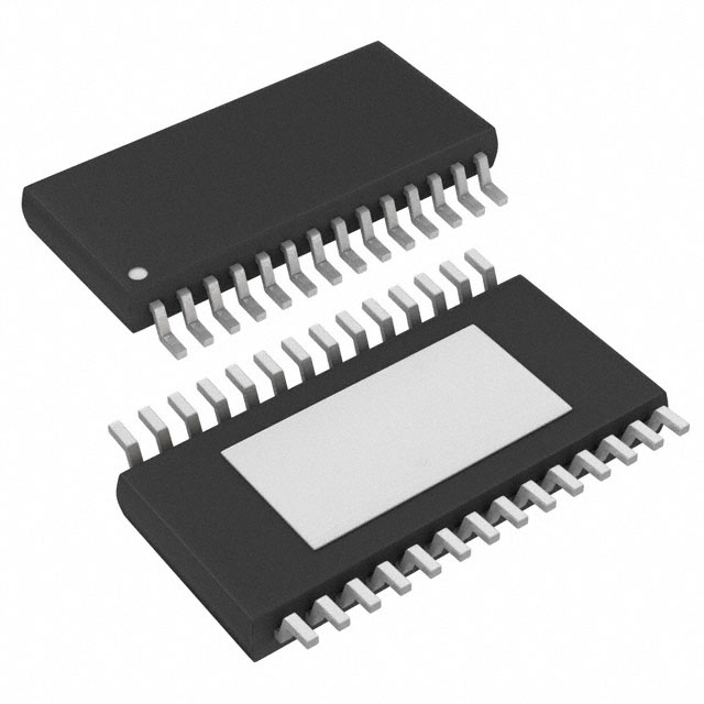
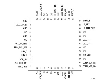
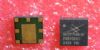
SKY74691: Features: • Three-step gain control, cellular LNA• External resistor to adjust LNA bias current• Buffered LO signal for transmit upconverter• VGA with 90 dB dynamic rangeR...
SeekIC Buyer Protection PLUS - newly updated for 2013!
268 Transactions
All payment methods are secure and covered by SeekIC Buyer Protection PLUS.
US $2.23 - 3.32 / Piece
Clock Synthesizer / Jitter Cleaner 2.1GHz 100Hz step Freq. Synthesizer
US $2.05 - 2.48 / Piece
Clock Synthesizer / Jitter Cleaner 2.1GHz 100Hz step Freq. Synthesizer
The SKY74691 is a highly integrated, super-heterodyne receiver. This single band receiver is intended for use in Code Division Multiple Access (CDMA) phones in cellular CDMA mode.
Except for the Surface Acoustic Wave (SAW) filters and matching components, the device incorporates all the components required to implement the receiver chain, from the Low-Noise Amplifier (LNA) to the In-Phase and Quadrature (I/Q) demodulator stages.
After RF LNA signal amplification and filtering from the antenna, the received signal of SKY74691 is downconverted from RF to the Intermediate Frequency (IF).
The LO_IN signal (pin 39) of SKY74691 provides a Local Oscillator (LO) port for the RF mixer. The UHF Voltage Controlled Oscillator (VCO) is buffered and amplified internally, and provides the LO to drive the LO port of a transmitter upconverter (such as Skyworks CX74002).
The Variable Gain Amplifier (VGA) SKY74691 has a minimum dynamic range of 90 dB with a control voltage range of 0.2 to 2.7 V. A VHF oscillator operates with an internal tank circuit to provide LO frequencies for the I/Q demodulator.
The noise figure, gain, and third order Input Intercept Point (IIP3) of each stage in the receiver SKY74691 are optimized to eet the system requirements for CDMA according to TIA/EIA-98-B/C.
The design of SKY74691 employs SiGe BiCMOS technology for low cost, high performance, and a high level of integration. The device package and pinout for the 48-pin RF Land Grid Array (RFLGA) are shown in Figure 1 and a block diagram of the SKY74691 is shown in Figure 2.