Features: • High efficiency
- GSM850 43%
- GSM900 43%
- DCS 40%
- PCS 40%
• Internal ICC sense-resistor for iPAC
• Closed loop iPAC or open loop operation with external PAC circuit
• Input/Output matching 50 ohms internal (with DC blocking)
• TX-VCO-to-antenna and antenna-to-RX-SAW filter RF interface
• TX harmonics below
33 dBm`
• PHEMT RF switches afford high linearity, low insertion loss and less than 20 A supply current in receive modes
• Small outline
- 8 mm x 10 mm
• Low profile
- 1.2 mm maximum
• Low APC current:
- 20 A
• Gold plated, lead free contacts
• High impedance control inputs, 15 A, typicalApplication• Quad-band cellular handsets comprised of
- Class 4 GSM850/900
- Class 1 DCS1800 PCS1900
- Class 12 GPRS multi-slot operationSpecifications
- High efficiency
- Internal ICC sense-resistor for PAC
- TX-VCO-to-antenna and Antenna-to-RX-SAW filter interface
- Closed loop iPAC? operation or open loop (external PAC)
- Low APC current,
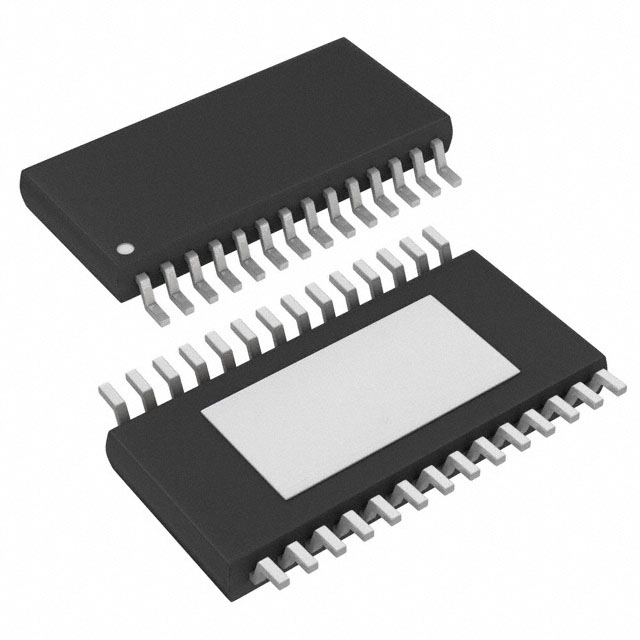
DescriptionTX-RX iPAC FEM Quad-Band GSM/GPRS GSM850, GSM900, DCS1800, PCS1900
The SKY77500 incorporates separate GSM850/900 andDCS1800/PCS1900 PA blocks that share a common power supplyinput for current distribution. Impedance-matching circuitry for50 input/output and a PA bias control block are alsoincorporated. Internal decoder circuitry controls the RF switchesand provides a low current external control interface. TheSKY77500 is packaged in a 32-pin, 8 x 10 mm Multi-Chip Module(MCM) package.
The SKY77500 is a transmit and receive Front End Module (FEM) designed in a low profile (1.2 mm), compact form factor for quad-band cellular handsets comprising GSM850/900, DCS1800, and PCS1900 operation-a complete transmit VCO-to-Antenna and Antenna-to-receive SAW filter solution. The FEM SKY77500 also supports Class 12 General Packet Radio Service (GPRS) multi-slot operation.
The module SKY77500 consists of separate GSM850/900 and DCS1800/PCS1900 PA blocks, internal circuitry for matching to 50 input and output impedances, TX harmonics filtering, high linearity and low insertion loss PHEMT RF switches, diplexer, and an integrated power amplifier control (iPAC™) function that utilizes an internal current-sense resistor. A custom silicon integrated circuit contains decoder circuitry to control the RF switches while providing a low current external control interface. Two Heterojunction Bipolar Transistor (HBT) PA blocks are fabricated onto a single Gallium Arsenide (GaAs) die; one supports the GSM850/900 bands and the other supports the DCS1800 and PCS1900 bands. Both PA blocks of SKY77500 share common power supply pins to distribute current. The output of each PA block and the outputs to the four receive pins are connected to the antenna pin through PHEMT RF switches and a diplexer. The GaAs die, PHEMT dies, Silicon (Si) die, and passive components are mounted on a multi-layer laminate substrate. The assembly of SKY77500 is encapsulated with plastic overmold. Band selection and control of transmit and receive RF signal flows are performed by use of three external control pins. See Figure 1 shown below. Two band select pins select GSM, DCS or PCS modes of operation and the TX_RX pin selects the receive or transmit mode of the respective RF switch (TX = logic 1). Proper timing of the logic on this pin, PAC Enable, and Analog Power Control (APC) of SKY77500 allow for high isolation between the antenna and TX-VCO while the VCO is being tuned prior to the transmit burst. The PAC Enable input allows initial turn-on of the PAC circuitry to minimize battery drain.

 SKY77500 Data Sheet