Features: State-of-the-Art Advanced BiCMOS Technology (ABT) Design for 3.3-V Operation and Low Static-Power Dissipation
Support Mixed-Mode Signal Operation (5-V Input and Output Voltages With 3.3-V VCC)
Support Unregulated Battery Operation Down to 2.7 V
Typical VOLP (Output Ground Bounce) < 0.8 V at VCC = 3.3 V, TA = 25°C
Ioff and Power-Up 3-State Support Hot Insertion
Bus Hold on Data Inputs Eliminates the Need for External Pullup/Pulldown Resistors
Latch-Up Performance Exceeds 500 mA Per JESD 17
ESD Protection Exceeds 2000 V Per MIL-STD-883, Method 3015; Exceeds 200 V Using Machine Model (C = 200 pF, R = 0)
Package Options Include Plastic Small-Outline (DW), Shrink Small-Outline (DB), and Thin Shrink Small-Outline (PW) Packages, Ceramic Chip Carriers (FK), and Ceramic (J) DIPs
Pinout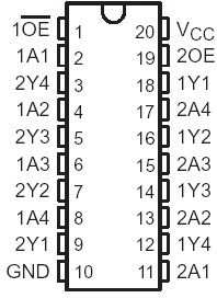 SpecificationsSupply voltage range, VCC . . . . . . . . . . . . . . . . . . . . . . . . . . . . . . . . . . . . . . . . . . . . .. . . .0.5 V to 4.6 V
Input voltage range, VI (see Note 1) . . . . . . . . . . . . . . . . . . . . . . . . . . . . . . . . . . . . . . . . . .0.5 V to 7 V
Voltage range applied to any output in the high-impedance
or power-off state, VO (see Note 1). . . . . . . . . . . . . . . . . . . . . . . . . . . . . . . . . . . . . . . . . 0.5 V to 7 V
Voltage range applied to any output in the high state, VO (see Note 1) . . . . . . . .0.5 V to VCC + 0.5 V
Current into any output in the low state, IO: SN54LVTH241 . . . . . . . . . . . . . . . . . . . . . .. . . . . . . .96 mA
SN74LVTH241 . . . . . . . . . . . . . . . . . . . . . . . . . . . .128 mA
Current into any output in the high state, IO (see Note 2): SN54LVTH241 . . . . . . . . . . . . . . . . . . .48 mA
SN74LVTH241 . . . . . . . . . . . . . . . . . . .64 mA
Input clamp current, IIK (VI < 0) . . . . . . . . . . . . . . . . . . . . . . . . . . . . . . . . . . . . . . . . . . . . . . . . . . .50 mA
Output clamp current, IOK (VO < 0) . . . . . . . . . . . . . . . . . . . . . . . . . . . . . . . . . . . . . . . . . . . . . . . . .50 mA
Package thermal impedance, JA (see Note 3): DB package . . . . . . . . . . . . . . . .. . . . . . . . .. . . .115°C/W
DW package . . . . . . . . . . . . . . . . . . . . . . . . . . . . .97°C/W
PW package . . . . . . . . . . . . . . . . . . . . . . . . . . . .128°C/W
Storage temperature range, Tstg . . . . . . . . . . . . . . . . . . . . . . . . . . . . . . . . . . . . . . . . . . . .65°C to 150°C DescriptionThese octal buffers/drivers of SN54LVTH241 are designed specifically for low-voltage (3.3-V) VCC operation, with the capability to provide a TTL interface to a 5-V system environment.
The 'LVTH241 devices are organized as two 4-bit line drivers with separate output-enable (1OE, 2OE) inputs. When 1OE is low or 2OE is high, the SN54LVTH241 pass noninverted data from the A inputs to the Y outputs. When 1OE is high or 2OE is low, the outputs of SN54LVTH241 are in the high-impedance state.
Active bus-hold circuitry of SN54LVTH241 is provided to hold unused or floating data inputs at a valid logic level.
When VCC is between 0 and 1.5 V, the SN54LVTH241 is in the high-impedance state during power up or power down. However, to ensure the high-impedance state above 1.5 V, OE should be tied to VCC through a pullup resistor SN54LVTH241 and OE should be tied to GND through a pulldown resistor; the minimum value of the resistor is determined by the current-sinking/current-sourcing capability of the driver.
SN54LVTH241 is fully specified for hot-insertion applications using Ioff and power-up 3-state. The Ioff circuitry disables the outputs, preventing damaging current backflow through the devices when they are powered down. The power-up 3-state circuitry of SN54LVTH241 places the outputs in the high-impedance state during power up and power down, which prevents driver conflict.
The SN54LVTH241 is characterized for operation over the full military temperature range of 55°C to 125°C. The SN74LVTH241 is characterized for operation from 40°C to 85°C.

 SN54LVTH241 Data Sheet


