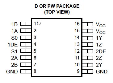
Features: · Designed for Signaling Rates (1) Up To 1.5 Gbps· Total Jitter < 65 ps· Pin-Compatible With SN65LVDS22 and SN65LVDM22· 25 mV of Receiver Input Threshold Hysteresis Over 0-V to 4-V Common-Mode Range· Inputs Electrically Compatible With CML, LVPECL and LVDS Signal Levels· Propagation D...
SN65LVDT122: Features: · Designed for Signaling Rates (1) Up To 1.5 Gbps· Total Jitter < 65 ps· Pin-Compatible With SN65LVDS22 and SN65LVDM22· 25 mV of Receiver Input Threshold Hysteresis Over 0-V to 4-V Comm...
SeekIC Buyer Protection PLUS - newly updated for 2013!
268 Transactions
All payment methods are secure and covered by SeekIC Buyer Protection PLUS.

|
SN65LVDS122, SN65LVDT122 | |||
| VCC Supply voltage range(2) |
0.5 V to 4 V | ||
| Voltage range | (A, B) |
0.7 V to 4.3 V | |
| |VA-VB| (LVDT only) |
1 V | ||
| (DE, S0, S1) |
0.5 V to 4 V | ||
| (Y, Z) |
0.5 V to 4 V | ||
| ESD | Human Body Model(3) | A, B, Y, Z, and GND |
±4 kV |
| All pins |
±2 kV | ||
| Charged-Device Model(4) | All pins |
±1500 V | |
| Continuous power dissipation |
See Dissipation Rating Table | ||
| Tstg Storage temperature range |
65°C to 150°C | ||
| Lead temperature 1,6 mm (1/16 inch) from case for 10 seconds |
260°C | ||
The SN65LVDS122 and SN65LVDT122 are crosspoint switches that use low voltage differential signaling (LVDS) to achieve signaling rates as high as 1.5 Gbps. They are pin-compatible speed up-grades to the SN65LVDS22 and SN65LVDM22. The internal signal paths maintain differential signaling for high speeds and low signal skews. SN65LVDS122 and SN65LVDT122 have a 0-V to 4-V common-mode input range that accepts LVDS, LVPECL, or CML inputs. Two logic pins (S0 and S1) set the internal configuration between the differential inputs and outputs. This allows the flexibility to perform the following configurations: 2 x 2 crosspoint switch, 2:1 input multiplexer, 1:2 splitter or dual repeater/translator within a single device. Additionally, SN65LVDT122 incorporates a 110- termination resistor for those applications where board space is a premium. Although SN65LVDS122 and SN65LVDT122 are designed for 1.5 Gbps, some applications at a 2-Gbps data rate can be supported depending on loading and signal quality.
The intended application of SN65LVDS122 and SN65LVDT122 is ideal for loopback switching for diagnostic routines, fanout buffering of clock/data distribution provide protection in fault-tolerant systems, clock multiplexing in optical modules, and for overall signal boosting over extended distances.
The SN65LVDS122 and SN65LVDT122 are characterized for operation from 40°C to 85°C.