Features: · Inputs Are TTL-Voltage Compatible
· EPICE (Enhanced-Performance Implanted CMOS) 1-mm Process
· 3-State Inverted Outputs Drive Bus Lines Directly
· Flow-Through Architecture to Optimize PCB Layout
· Full Parallel Access for Loading
· Package Options Include Plastic Small-Outline (DW), Shrink Small-Outline (DB), Thin Shrink Small-Outline (PW), Ceramic Chip Carriers (FK) and Flatpacks (W), and Standard Plastic (N) and Ceramic (J) DIPs
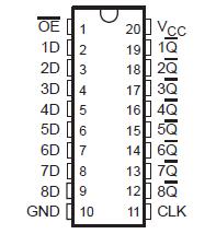
Pinout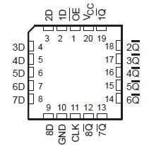
 Specifications
Supply voltage range, VCC . . . . . . . . . . . . . . . . . . . . . . . . . . . . . . . . . . . . . 0.5 V to 7 V
Input voltage range, VI (see Note 1) . . . . . . . . . . . . . . . . . . . . . . 0.5 V to VCC + 0.5 V
Output voltage range, VO (see Note 1) . . . . . . . . . . . . . . . . . . . . . 0.5 V to VCC + 0.5 V
Input clamp current, IIK (VI < 0 or VI > VCC) . . . . . . . . . . . . . . . . . . . . . . . . . . . . ±20 mA
Output clamp current, IOK (VO < 0 or VO > VCC) . . . . . . . . . . . . . . . . . . . . .. . . . . ±20 mA
Continuous output current, IO (VO = 0 to VCC) . . . . . . . . . . . . . . . . . . . . .. . . . . . ±50 mA
Continuous current through VCC or GND . . . . . . . . . . . . . . . . . . . . . . . . . .. . . . . ±200 mA
Maximum power dissipation at TA = 55°C (in still air) (see Note 2): DB package .. . 0.6 W
DW package . . 1.6 W
N package . . . 1.3 W
PW package . . 0.7 W
Storage temperature range, Tstg . . . . . . . . . . . . . . . . . . . . . . . . . . . . . . 65°C to 150°C
‡ Stresses beyond those listed under "absolute maximum ratings" may cause permanent damage to the device. These are stress ratings only, and functional operation of the device at these or any other conditions beyond those indicated under "recommended operating conditions" is not implied. Exposure to absolute-maximum-rated conditions for extended periods may affect device reliability.
NOTES: 1. The input and output voltage ratings may be exceeded if the input and output current ratings are observed.
2. The maximum package power dissipation is calculated using a junction temperature of 150°C and a board trace length of 750 mils, except for the N package, which has a trace length of zero.
DescriptionThe 'ACT564 are octal D-type edge-triggered flip-flops that feature 3-state outputs designed specifically for driving highly capacitive or relatively low-impedance loads. They are particularly suitable for implementing buffer registers, I/O ports, bidirectional bus drivers, and working registers.
On the positive transition of the clock (CLK) input, the Q outputs are set to the complements of the logic levels set up at the data (D) inputs. A buffered output-enable (OE) input places the eight outputs in either a normal logic state (high or low logic levels) or the high-impedance state. In the high-impedance state, the outputs neither load nor drive the bus lines significantly. The high-impedance state and increased drive of 'ACT564 provide the capability to drive bus lines without interface or pullup components. OE does not affect internal operations of the flip-flops. Old data can be retained or new data can be entered
while the outputs are in the high-impedance state.The SN54ACT564 is characterized for operation over the full military temperature range of 55°C to 125°C. The
SN74ACT564 is characterized for operation from 40°C to 85°C.

 SN74ACT564 Data Sheet


