Pinout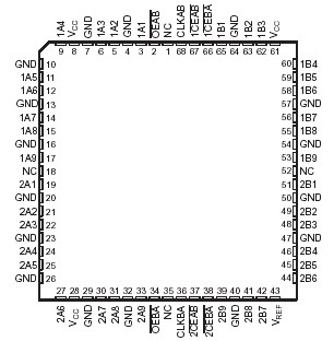 Specifications
Supply voltage range, VCC . . . . . . . . . . . . . . . . . . . . . . . . . . . . . . . . . . . . . . . . . . . . . . . . .0.5 V to 4.6 V
Input voltage range, VI (see Note 1): A port/B port . . . . . . . . . . . . . . . . . . . . . . . . . . . . . .0.5 V to 4.6 V
Voltage range applied to any output in the high or power-off state, VO
(see Note 1): A port/B port . . . . . . . . . . . . . . . . . . . . . . . . . . . . . . . . . . . . . . . . . . . . . .0.5 V to 4.6 V
Current into any output in the low state, IO: A port . . . . . . . . . . . . . . . . . . . . . . . . . . . . . . . . . . . .48 mA
B port . . . . . . . . . . . . . . . . . . . . . . . . . . . . . . . . . . .100 mA
Input clamp current, IIK (VI < 0) . . . . . . . . . . . . . . . . . . . . . . . . . . . . . . . . . . . . . .. . . . . . . . . . . . .50 mA
Output clamp current, IOK (VO < 0) . . . . . . . . . . . . . . . . . . . . . . . . . . . . . . . . . . . . . . . . . . . . . . . .50 mA
Maximum power dissipation at TA = 55°C (in still air) (see Note 2): DGG package . . . . .. . . . . . . . .1.3 W
Storage temperature range, Tstg . . . . . . . . . . . . . . . . . . . . . . . . . . . . . . . . . . . . . . . . . . .65°C to 150°C
DescriptionThese SN74GTL16622 18-bit registered bus transceivers contain two sets of D-type flip-flops for temporary storage of data flowing in either direction.
The SN74GTL16622 B port operates at GTL (VTT = 1.2 V and VREF = 0.8 V) and GTL+ (VTT = 1.5 V and VREF = 1 V) levels, while the A port and control inputs are compatible with LVTTL logic levels.
Data flow in each direction is controlled by output-enable (OEAB and OEBA) and clock (CLKAB and CLKBA) inputs. The clock-enable (CEAB and CEBA) inputs are designed to control each 9-bit transceiver independently, which makes the device more versatile.
For A-to-B data flow, the SN74GTL16622 devices operate on the low-to-high transition of CLKAB if CEAB is low. When OEAB is low, the outputs are active. When OEAB is high, the outputs are in the high-impedance state. Data flow for B to A is similar to that for A to B, but uses OEBA, CLKBA, and CEBA.
SN74GTL16622 Active bus-hold circuitry is provided to hold unused or floating TTL inputs at a valid logic state.
To ensure the high-impedance state during SN74GTL16622 power up or power down, OE should be tied to VCC through a pullup resistor; the minimum value of the resistor is determined by the current-sinking capability of the driver.
The SN54GTL16622 is characterized for operation over the full military temperature range of 55°C to 125°C. The SN74GTL16622 is characterized for operation from 40°C to 85°C.

 SN74GTL16622 Data Sheet


