SP5611

Features: Complete 1`3GHz Single Chip SystemHigh Sensitivity RF InputsProgrammable via I2C BUSLow Power Consumption (5V, 20mA)Low RadiationPhase Lock DetectorVaractor Drive Amp Disable4 Bi-directional Controllable Outputs5-Level ADCVariable I2C BUS Address for Multi-tuner ApplicationsESD Protectio...

product image

SP5611 Picture
SeekIC No. : 004500498 Detail

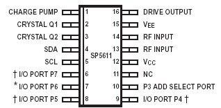
SP5611: Features: Complete 1`3GHz Single Chip SystemHigh Sensitivity RF InputsProgrammable via I2C BUSLow Power Consumption (5V, 20mA)Low RadiationPhase Lock DetectorVaractor Drive Amp Disable4 Bi-direction...

floor Price/Ceiling Price

Part Number:
SP5611
Supply Ability:
5000

Price Break

  • Qty
  • 1~5000
  • Unit Price
  • Negotiable
  • Processing time
  • 15 Days
Total Cost: $ 0.00

SeekIC Buyer Protection PLUS - newly updated for 2013!

  • Escrow Protection.
  • Guaranteed refunds.
  • Secure payments.
  • Learn more >>

Month Sales

268 Transactions

Rating

evaluate  (4.8 stars)

Upload time: 2025/12/24

Payment Methods

All payment methods are secure and covered by SeekIC Buyer Protection PLUS.

Notice: When you place an order, your payment is made to SeekIC and not to your seller. SeekIC only pays the seller after confirming you have received your order. We will also never share your payment details with your seller.
Product Details

Description


Features:

 Complete 1`3GHz Single Chip System
 High Sensitivity RF Inputs
 Programmable via I2C BUS
 Low Power Consumption (5V, 20mA)
 Low Radiation
 Phase Lock Detector
 Varactor Drive Amp Disable
 4 Bi-directional Controllable Outputs
 5-Level ADC
 Variable I2C BUS Address for Multi-tuner Applications
 ESD Protection: 4kV, Mil-Std-883C, Method 3015 (1)
 Switchable 4512/1024 Reference Divider
 Pin and Function Compatible with SP5511S (2)


Application

 Satellite TV
 Cable Tuning Systems
 VCRs


Pinout

  Connection Diagram


Specifications

Parameter
Pin
Value
Units
Conditions
Min
Max
Supply voltage
RF input voltage
RF input DC offset
Port voltage
Total port current

ADC input DC offset
REF/COMP output DC offset
Charge pump DC offset
Drive DC offset
Crystal oscillator DC offset
Address DC offset
SDA, SCL input voltage

Storage temperature
Junction temperature

12
13,14
6-9
6-9
6-9
10
13-14
1
16
2
4,5


-0·3


-0·3
-0·3

-0·3
-0·3
-0·3
-0·3
-0·3
-0·3
-0·3
-55

7
2·5
14
6
50
VCC+0·3
VCC+0·3
VCC+0·3
VCC+0·3
VCC+0·3
VCC+0·3
6
+150
+150
V
V p-p
V
V
V
mA
V
V
V
V
V
V
V
°C
°C


Port in off state
Port in on state


Customers Who Bought This Item Also Bought

Margin,quality,low-cost products with low minimum orders. Secure your online payments with SeekIC Buyer Protection.
Resistors
Audio Products
Connectors, Interconnects
Line Protection, Backups
Optical Inspection Equipment
Cables, Wires - Management
View more