Features: Complete 2`7GHz Single Chip SystemOptimised for Low Phase NoiseSelectable ÷2 prescalerSelectable Reference Division RatioSelectable Reference/Comparison Frequency OutputSelectable Charge Pump CurrentVaractor Drive Amplifier Disable5-Level ADCVariable I2C BUS Address for Multi-tuner Appli...
SP5659: Features: Complete 2`7GHz Single Chip SystemOptimised for Low Phase NoiseSelectable ÷2 prescalerSelectable Reference Division RatioSelectable Reference/Comparison Frequency OutputSelectable Charge P...
SeekIC Buyer Protection PLUS - newly updated for 2013!
268 Transactions
All payment methods are secure and covered by SeekIC Buyer Protection PLUS.


|
Parameter |
Pin |
Value |
Units |
Conditions | |
|
Min |
Max | ||||
|
Supply voltage RF input voltage RF input DC offset Port voltage Total port current ADC input DC offset REF/COMP output DC offset Charge pump DC offset Drive DC offset Crystal oscillator DC offset Address DC offset SDA, SCL input voltage Storage temperature Junction temperature |
12 13,14 13, 14 7-10 7-10 7-10 11 3 1 16 2 4 5, 6 |
-0·3 -0·3 -0·3 -0·3 -0·3 -0·3 -0·3 -0·3 -0·3 -0·3 -55 |
7 2·5 14 6 14 50 VCC+0·3 VCC+0·3 VCC+0·3 VCC+0·3 VCC+0·3 5·5 +150 +150 |
V V p-p V V V mA V V V V V V V °C °C |
Port in off state Port in on state |
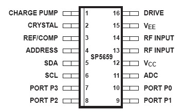
The SP5659 is designed as one kind of single chip frequency synthesiser which can be disabled for applications up to 2GHz, allowing direct interfacing with the programmable divider, resulting in a step size equal to the comparison frequency.And it contains a varactor line disable and charge pump disable facility.The SP5659 can be used in satellite TV and high IF cable tuning systems.
Features of the SP5659 are:(1)pin compatible with SP5658;(2)ESD protection: 4kV, Mil-Std-883C, Method 3015;(3)5-level ADC;(4)varactor drive amplifier disable;(5)selectable charge pump current;(6)selectable reference/comparison frequency output;(7)selectable reference division ratio;(8)optimised for low phase noise;(9)complete 2.7GHz single chip system.
The absolute maximum ratings of the SP5659 can be summarized as:(1)supply voltage:-0.3 to 7 V;(2)RF input voltage:2.5 Vp-p;(3)RF input DC offset:Vcc+ 0.3 V;(4)port voltage:-0.3 to 14 V;(5)junction temperature:+150 °C;(6)storage temperature:-55 to +150 °C;(7)SDA, SCL input voltage:-0.3 to 6 V;(8)address DC offset:-0.3 to Vcc+0.3 V;(9)crystal oscillator DC offset:-0.3 to Vcc+0.3 V;(10)drive DC offset:-0.3 to Vcc+0.3 V;(11)charge pump DC offset:-0.3 to Vcc+0.3 V;(12)REF/COMP output DC offset:-0.3 to Vcc+0.3 V;(13)ADC input DC offset:-0.3 to Vcc+0.3 V.If you want to know more information such as the electrical characteristics about the SP5659,please download the datasheet in www.seekic.com or www.chinaicmart.com .