SP5769

Features: Complete 3`0 GHz Single Chip System Optimised for Low Phase Noise, with Comparison Frequencies up to 4 MHz No RF Prescaler Selectable Reference Division Ratio Selectable Reference/Comparison Frequency Output Selectable Charge Pump Current with 10:1 Ratio Four Selectable I2C Addresses I2...

product image

SP5769 Picture
SeekIC No. : 004500510 Detail

SP5769: Features: Complete 3`0 GHz Single Chip System Optimised for Low Phase Noise, with Comparison Frequencies up to 4 MHz No RF Prescaler Selectable Reference Division Ratio Selectable Reference/Compari...

floor Price/Ceiling Price

Part Number:
SP5769
Supply Ability:
5000

Price Break

  • Qty
  • 1~5000
  • Unit Price
  • Negotiable
  • Processing time
  • 15 Days
Total Cost: $ 0.00

SeekIC Buyer Protection PLUS - newly updated for 2013!

  • Escrow Protection.
  • Guaranteed refunds.
  • Secure payments.
  • Learn more >>

Month Sales

268 Transactions

Rating

evaluate  (4.8 stars)

Upload time: 2025/12/24

Payment Methods

All payment methods are secure and covered by SeekIC Buyer Protection PLUS.

Notice: When you place an order, your payment is made to SeekIC and not to your seller. SeekIC only pays the seller after confirming you have received your order. We will also never share your payment details with your seller.
Product Details

Description


Features:

Complete 3`0 GHz Single Chip System
Optimised for Low Phase Noise, with Comparison Frequencies up to 4 MHz
No RF Prescaler
Selectable Reference Division Ratio
Selectable Reference/Comparison Frequency Output
Selectable Charge Pump Current with 10:1 Ratio
Four Selectable I2C Addresses
I2C Fast Mode Compliant with 3`3V and 5V Logic Levels
Four Switching Ports
Functional Replacement for SP5659 (except ADC)
Pin Compatible with SP5655
Power Consumption 110mW with VCC = 5`5V, all Ports off
ESD Protection 2kV min., MIL-STD-883B Method 3015 Cat.1 (Normal ESD handling procedures should be observed)


Application

 Digital Satellite and Cable Tuning Systems
 Communications Systems


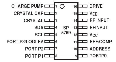
Pinout

  Connection Diagram


Specifications

All voltages are referred to VEE = 0V
Supply voltage, VCC
RF differential input voltage
All I/O port DC offsets
SDA and SCL DC offset
Storage temperature
Junction temperature
MP16 thermal resistance
Chip to ambient, JA
Chip to case, JC

0`3V to 17V
2`5Vp-p
20`3 to VCC 10`3V
20`3 to 6V
255°C to 1125°C
1150°C

80°C/W
20°C/W


Customers Who Bought This Item Also Bought

Margin,quality,low-cost products with low minimum orders. Secure your online payments with SeekIC Buyer Protection.
Soldering, Desoldering, Rework Products
Hardware, Fasteners, Accessories
Integrated Circuits (ICs)
Optical Inspection Equipment
Discrete Semiconductor Products
View more