STP12NB30FP

DescriptionThe STP12NB30FP is designed as one kind of N-channel enhancement mode powerMESH MOSFETs. Using the latest high voltage MESH OVERLAY process, SGS-Thomson has designed an advanced family of power MOSFETs with outstanding performances. The new patent pending strip layout coupled with the c...

product image

STP12NB30FP Picture
SeekIC No. : 004508325 Detail

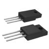
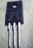
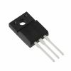
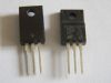
STP12NB30FP: DescriptionThe STP12NB30FP is designed as one kind of N-channel enhancement mode powerMESH MOSFETs. Using the latest high voltage MESH OVERLAY process, SGS-Thomson has designed an advanced family of...

floor Price/Ceiling Price

Part Number:
STP12NB30FP
Supply Ability:
5000

Price Break

  • Qty
  • 1~5000
  • Unit Price
  • Negotiable
  • Processing time
  • 15 Days
Total Cost: $ 0.00

SeekIC Buyer Protection PLUS - newly updated for 2013!

  • Escrow Protection.
  • Guaranteed refunds.
  • Secure payments.
  • Learn more >>

Month Sales

268 Transactions

Rating

evaluate  (4.8 stars)

Upload time: 2025/12/24

Payment Methods

All payment methods are secure and covered by SeekIC Buyer Protection PLUS.

Notice: When you place an order, your payment is made to SeekIC and not to your seller. SeekIC only pays the seller after confirming you have received your order. We will also never share your payment details with your seller.
Product Details

Description


Description

The STP12NB30FP is designed as one kind of N-channel enhancement mode powerMESH MOSFETs. Using the latest high voltage MESH OVERLAY process, SGS-Thomson has designed an advanced family of power MOSFETs with outstanding performances. The new patent pending strip layout coupled with the company's proprietary edge termination structure, gives the lowest RDS(on) per area, exceptional avalanche and dv/dt capabilities and unrivalled gate charge and switching characteristics.

STP12NB30FP has five features. (1)Typical Rds(on) is 0.34ohms. (2)Extremely high dv/dt capability. (3)100% avalanche tested. (4)Very low intrinsic capacitances. (5)Gate charge minimized. Those are all the main features.

Some STP12NB30FP absolute maximum ratings have been concluded into several points as follow. (1)Its drain to source voltage would be 300V. (2)Its drain to gate voltage would be 300V. (3)Its gate to source voltage would be +/-30V. (4)Its drain current continuous would be 6.5V at Tc=25°C and would be 4A at Tc=100°C. (5)Its drain current pulsed would be 48A. (6)Its total dissipation at Tc=25°C would be 35W. (7)Its derating factor would be 0.28W/°C. (8)Its peak diode recovery voltage slope would be 5.5V/ns. (9)Its insulation withstand voltage DC would be 2000V. (10)Its storage temperature range would be from -65°C to 150°C. (11)Its max operating junction temperature would be 150°C. It should be noted that stresses above those listed in absolute maximum ratings may cause permanent damage to device.

Also some STP12NB30FP electrical characteristics are concluded as follow. (1)Its drain to source breakdown voltage would be min 300V. (2)Its zero gate voltage drain current (Vgs=0) would be max 1uA and would be max 10uA at Tc=100°C. (3)Its gate to body leakage current Vds=0 would be max +/-100nA. And so on. At present we have not got so much information about this IC and we would try hard to get more information about it. If you have any question or suggestion or want to know more information please contact us for details. Thank you!


Customers Who Bought This Item Also Bought

Margin,quality,low-cost products with low minimum orders. Secure your online payments with SeekIC Buyer Protection.
Undefined Category
Optical Inspection Equipment
Line Protection, Backups
Isolators
Semiconductor Modules
View more