Features: Fast Access times: 4.5, 5, 6, 7, and 8ns
Fast clock speed: 125,100, 83, 66, and 50 MHz
Provide high performance 3-1-1-1 access rate
Fast OE access times: 4.5, 5 and 6ns
Single 3.3V +10%/-5% power supply
Common data inputs and data outputs
BYTE WRITE ENABLE and GLOBAL WRITE control
Three chip enables for depth expansion and address pipelining
Address, control, input, and output pipelined registers
Internally self-timed WRITE CYCLE
WRITE pass-through capability
Burst control pins ( interleaved or linear burst sequence)
High density, high speed packages
Low capacitive bus loading
High 30pF output drive capability at rated access time
SNOOZE MODE for reduced power standby
Single cycle disable ( PentiumTM BSRAM compatible )
Pinout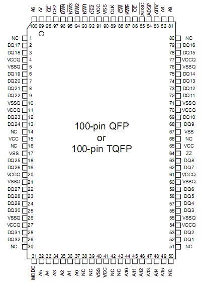 Specifications
Voltage on VCC Supply Relative to VSS.
....-0.5V to +4.6V
I/O Supply Voltage VccQ ................. Vss -0.5V to Vcc
VIN....................................... -0.5V to Vcc +0.5V
Storage Temperature (plastic)............ -55 to +150
Junction Temperature ............................... +150
Power Dissipation ..................................... 1.6W
Short Circuit Output Current......................... 100mA
DescriptionThe Taiwan Memory Technology Synchronous Burst RAM T35L6432A family employs high-speed, low power CMOS design using advanced triple-layer polysilicon,double-layer metal technology. Each memory cell consists of four transistors and two high valued resistors.
The T35L6432A SRAM integrates 65536 x 32 SRAM cells with advanced synchronous peripheral circuitry and a 2-bit counter for internal burst operation. All synchronous inputs are gated by registers controlled by a positive-edge-triggered clock input (CLK). The synchronous inputs of T35L6432A include all addresses, all data inputs, address-pipelining chip enable ( CE ), depth-expansion chip enables (CE2 and CE2), burst control inputs (ADSC , ADSP , and ADV ), write enables (BW1 , BW2 , BW3 , BW4 , and BWE ), and global write (GW ).
Asynchronous inputs of T35L6432A include the output enable (OE ), Snooze enable (ZZ) and burst mode control (MODE). The data outputs (Q), enabled by OE , are also asynchronous.
Addresses and chip of T35L6432A enables are registered with either address status processor (ADSP ) or address status controller (ADSC ) input pins. Subsequent burst addresses can be internally generated as controlled by the burst advance pin (ADV ).
Address and write controls T35L6432A are registered on-chip to initiate self-timed WRITE cycle. WRITE cycles can be one to four bytes wide as controlled by the write control inputs. Individual byte write allows individual byte to be written. BW1 controls DQ1-DQ8. BW2 controls DQ9-DQ16. BW3 controls DQ17-DQ 24. BW4 controls DQ25-DQ32. BW1 , BW2 , BW3 , and BW4 can be active only with BWE being LOW. GW being LOW causes all bytes to be written. WRITE pass-through capability allows written data of T35L6432A available at the output for the immediately next READ cycle. T35L6432A also incorporates pipelined enable circuit for easy depth expansion without penalizing system performance.

 T35L6432A Data Sheet


