TPD1030F

Features: • Two built-in power IC chips with a new structure combining a control block and a vertical power MOSFET (L2--MOS) on each chip.• Can directly drive a power load from a CMOS or TTL logic.• Built-in protection circuits against overvoltage (active clamp), overtemperature ...

product image

TPD1030F Picture
SeekIC No. : 004526267 Detail

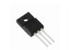
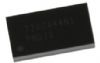
TPD1030F: Features: • Two built-in power IC chips with a new structure combining a control block and a vertical power MOSFET (L2--MOS) on each chip.• Can directly drive a power load from a CMOS or...

floor Price/Ceiling Price

Part Number:
TPD1030F
Supply Ability:
5000

Price Break

  • Qty
  • 1~5000
  • Unit Price
  • Negotiable
  • Processing time
  • 15 Days
Total Cost: $ 0.00

SeekIC Buyer Protection PLUS - newly updated for 2013!

  • Escrow Protection.
  • Guaranteed refunds.
  • Secure payments.
  • Learn more >>

Month Sales

268 Transactions

Rating

evaluate  (4.8 stars)

Upload time: 2024/4/26

Payment Methods

All payment methods are secure and covered by SeekIC Buyer Protection PLUS.

Notice: When you place an order, your payment is made to SeekIC and not to your seller. SeekIC only pays the seller after confirming you have received your order. We will also never share your payment details with your seller.
Product Details

Description


Features:

• Two built-in power IC chips with a new structure combining a control block and a vertical power MOSFET (L2--MOS) on each chip.
• Can directly drive a power load from a CMOS or TTL logic.
• Built-in protection circuits against overvoltage (active clamp), overtemperature (thermal shutdown), and overcurrent (current limiter).
• Low Drain-Source ON-resistance: R DS (ON) = 0.6 (max) (@VIN = 5 V, ID = 0.5 A, Tch = 25)
• Low Leakage Current: IDSS = 10 A (max) (@VIN = 0 V, VDS = 30 V, Tch = 25)
• Low Input Current: IIN = 300 A (max) (@VIN = 5 V, Tch = 25)
• 8-pin SOP package with embossed-tape packing.


Pinout

  Connection Diagram


Specifications

Characteristics
Symbol
Rating
Unit
Drain-source voltage
V DS(DC)
40
V
Drain current
ID
Internally Limited
A
Input voltage
VIN
−0.3 to 7
V
Power dissipation (t = 10 s)
PD
2.0 (Note 3)
W
Single pulse active clamp capability
(Note 4)
EAS
10
mJ
Active clamp current
IAR
1
A
Repetitive active clamp capability
(Note 5)
EAR
0.2
mJ
Operating temperature
Topr
−40 to 110
Channel temperature
Tch
150
Storage temperature
Tstg
−55 to 150

Note: Using continuously under heavy loads (e.g. the application of high temperature/current/voltage and the significant change in temperature, etc.) may cause this product to decrease in the reliability significantly even if the operating conditions (i.e. operating temperature/current/voltage, etc.) are within the absolute maximum ratings and the operating ranges.

Please design the appropriate reliability upon reviewing the Toshiba Semiconductor Reliability Handbook ("Handling Precautions"/Derating Concept and Methods) and individual reliability data (i.e. reliability test report and estimated failure rate, etc).


Customers Who Bought This Item Also Bought

Margin,quality,low-cost products with low minimum orders. Secure your online payments with SeekIC Buyer Protection.
Computers, Office - Components, Accessories
Potentiometers, Variable Resistors
Static Control, ESD, Clean Room Products
Soldering, Desoldering, Rework Products
Memory Cards, Modules
View more