Pinout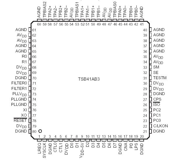 SpecificationsSupply voltage range, VDD (see Note 1) . . . . . . . . . . . . . . . . . . . . . . . . . . . . . . .0.3 V to 4 V
Input voltage range, VI (see Note 1) . . . . . . . . . . . . . . . . . . . . . . . . . . . . .0.5 V to VDD+0.5 V
5-V tolerant I/O supply voltage range, VDD . . . . . . . . . . . . . . . . . . . . . . . . .-5V 0.3 V to 5.5 V
5-V tolerant input voltage range, VI-5V . . . . . . . . . . . . . . . . . . . . . . . .0.5 V to VDD-5V+0.5 V
Output voltage range at any output, VO . . . . . . . . . . . . . . . . . . . . . . . . . .0.5 V to VDD+0.5 V
Continuous total power dissipation . . . . . . . . . . . . . . . . . . . . . . .See Dissipation Rating Table
Operating free air temperature, TA 0 . . . . . . . . . . . . . . . . . . . . . . . . . . . . . . . . . . . .°C to 70°C
Storage temperature range, Tstg . . . . . . . . . . . . . . . . . . . . . . . . . . . . .. . . . .65°C to 150°C
Lead temperature 1,6 mm (1/16 inch) from case for 10 seconds . . . . . . . . . . . . . .. . . . .260°C
NOTES: 1. All voltage values, except differential I/O bus voltages, are with respect to network ground.DescriptionThe TSB41AB3 provides the digital and analog transceiver functions needed to implement a three-port node in a cable-based IEEE 1394 network. Each cable port incorporates two differential line transceivers. The transceivers include circuitry to monitor the line conditions as needed for determining connection status, for initialization and arbitration, and for packet reception and transmission. The TSB41AB3 is designed to interface with a line layer controller (LLC), such as the TSB12LV21, TSB12LV22, TSB12LV23, TSB12LV26, TSB12LV31, TSB12LV41, TSB12LV42, or TSB12LV01A.
The TSB41AB3 requires only an external 24.576 MHz crystal as a reference. An external clock may be provided instead of a crystal. An internal oscillator drives an internal phase-locked loop (PLL), which generates the required 393.216 MHz reference signal. This reference signal is internally divided to provide the clock signals used to control transmission of the outbound encoded strobe and data information. A 49.152 MHz clock signal is supplied to the associated LLC for synchronization of the two chips and is used for resynchronization of the received data. The power-down (PD) function, when enabled by asserting the PD terminal high, stops operation of the PLL.
The TSB41AB3 supports an optional isolation barrier between itself and its LLC. When the ISO input terminal is tied high, the LLC interface outputs behave normally. When the ISO terminal is tied low, internal differentiating logic is enabled, and the outputs are driven such that they can be coupled through a capacitive or transformer galvanic isolation barrier as described in Annex J of IEEE Std 1394-1995 and in the 1394a-2000 Supplement (section 5.9.4) (hereafter referred to as Annex J type isolation). To operate with TI bus holder isolation, the ISO terminal on the PHY must be high.
Data bits to be transmitted through the cable ports are received from the LLC on two, four, or eight parallel paths (depending on the requested transmission speed). They are latched internally in the TSB41AB3 in synchronization with the 49.152-MHz system clock. These bits are combined serially, encoded, and transmitted at 98.304, 196.608, or 392.216 Mbits/s (referred to as S100, S200, and S400 speed respectively) as the outbound data-strobe information stream. During transmission, the encoded data information is transmitted differentially on the TPB cable pair(s), and the encoded strobe information is transmitted differentially on the TPA cable pair(s).
During packet reception the TPA and TPB transmitters of the receiving cable port are disabled, and the receivers for that port are enabled. The encoded data information is received on the TPA cable pair, and the encoded strobe information is received on the TPB cable pair. The received data-strobe information is decoded to recover the receive clock signal and the serial data bits. The TSB41AB3 serial data bits are split into two-, four-, or eight-bit parallel streams (depending upon the indicated receive speed), resynchronized to the local 49.152-MHz system clock and sent to the associated LLC. The received data is also transmitted (repeated) on the other active (connected)
cable ports.
Both the TPA and TPB cable interfaces incorporate differential comparators to monitor the line states during initialization and arbitration. The outputs of these comparators are used by the internal logic to determine the arbitration status. The TPA channel monitors the incoming cable common-mode voltage. The value of this common-mode voltage is used during arbitration to set the speed of the next packet transmission. In addition, the TPB channel monitors the incoming cable common-mode voltage on the TPB pair for the presence of the remotely supplied twisted-pair bias voltage.
The TSB41AB3 provides a 1.86-V nominal bias voltage at the TPBIAS terminal for port termination. The PHY contains three independent TPBIAS circuits. This bias voltage, when seen through a cable by a remote receiver, indicates the presence of an active connection. This bias voltage source must be stabilized by an external filter capacitor of 1 mF.
The line drivers in the TSB41AB3, operating in a high-impedance current mode, are designed to work with external 112-W line-termination resistor networks in order to match the 110-W cable impedance. One network is provided at each end of a twisted-pair cable. Each network is composed of a pair of series-connected 56-W resistors. The midpoint of the pair of resistors that is directly connected to the twisted-pair A terminals is connected to its corresponding TPBIAS voltage terminal. The midpoint of the pair of resistors that is directly connected to the twisted-pair B terminals is coupled to ground through a parallel R-C network with recommended values of 5 kW and 220 pF. The values of the external line-termination resistors TSB41AB3 are designed to meet the standard specifications when connected in parallel with the internal receiver circuits. An external resistor connected between the R0 and R1 terminals sets the driver output current, along with other internal operating currents. This current setting resistor has a value of 6.34 kW ±1%.

 TSB41AB3 Data Sheet