XC18V02

Features: • In-System Programmable 3.3V PROMs for Configuration of Xilinx FPGAs` Endurance of 20,000 Program/Erase Cycles` Program/Erase Over Full Industrial Voltage and Temperature Range (40°C to +85°C)• IEEE Std 1149.1 Boundary-Scan (JTAG) Support• JTAG Command Initiation of ...

product image

XC18V02 Picture
SeekIC No. : 004547721 Detail

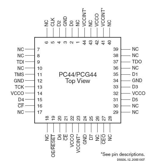
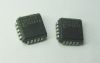
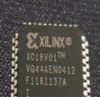
XC18V02: Features: • In-System Programmable 3.3V PROMs for Configuration of Xilinx FPGAs` Endurance of 20,000 Program/Erase Cycles` Program/Erase Over Full Industrial Voltage and Temperature Range (4...

floor Price/Ceiling Price

Part Number:
XC18V02
Supply Ability:
5000

Price Break

  • Qty
  • 1~5000
  • Unit Price
  • Negotiable
  • Processing time
  • 15 Days
Total Cost: $ 0.00

SeekIC Buyer Protection PLUS - newly updated for 2013!

  • Escrow Protection.
  • Guaranteed refunds.
  • Secure payments.
  • Learn more >>

Month Sales

268 Transactions

Rating

evaluate  (4.8 stars)

Upload time: 2024/4/22

Payment Methods

All payment methods are secure and covered by SeekIC Buyer Protection PLUS.

Notice: When you place an order, your payment is made to SeekIC and not to your seller. SeekIC only pays the seller after confirming you have received your order. We will also never share your payment details with your seller.
Product Details

Description


Features:

• In-System Programmable 3.3V PROMs for
   Configuration of Xilinx FPGAs
` Endurance of 20,000 Program/Erase Cycles
` Program/Erase Over Full Industrial Voltage and
   Temperature Range (40°C to +85°C)
• IEEE Std 1149.1 Boundary-Scan (JTAG) Support
• JTAG Command Initiation of Standard FPGA Configuration
• Simple Interface to the FPGA
• Cascadable for Storing Longer or Multiple Bitstreams
• Low-Power Advanced CMOS FLASH Process
• Dual Configuration Modes
` Serial Slow/Fast Configuration (up to 33 MHz)
` Parallel (up to 264 Mb/s at 33 MHz)
• 5V-Tolerant I/O Pins Accept 5V, 3.3V and 2.5V Signals
• 3.3V or 2.5V Output Capability
• Design Support Using the Xilinx ISE™ Foundation™
   Software Packages
• Available in PC20, SO20, PC44, and VQ44 Packages
• Lead-Free (Pb-Free) Packaging


Pinout

  Connection Diagram


Specifications

Symbol Description Value Units
VCCINT/VCCO Supply voltage relative to GND 0.5 to +4.0 V
VIN Input voltage with respect to GND 0.5 to +5.5 V
VTS Voltage applied to high-Z output 0.5 to +5.5 V
TSTG Storage temperature (ambient) 65 to +150 °C
TJ Junction temperature +125 °C
Notes:
1. Maximum DC undershoot below GND must be limited to either 0.5V or 10 mA, whichever is easier to achieve. During transitions, the device
pins can undershoot to 2.0V or overshoot to +7.0V, provided this over- or undershoot lasts less then 10 ns and with the forcing current being
limited to 200 mA.
2. Stresses beyond those listed under Absolute Maximum Ratings might cause permanent damage to the device. These are stress ratings
only, and functional operation of the device at these or any other conditions beyond those listed under Operating Conditions is not implied.
Exposure to Absolute Maximum Ratings conditions for extended periods of time might affect device reliability.


Description

Xilinx introduces the XC18V00 series of in-systemprogrammable configuration PROMs (Figure 1). Devices in this 3.3V family include a 4-megabit, a 2-megabit, a 1-megabit, and a 512-kilobit PROM that provide an easy-touse, cost-effective method for reprogramming and storing Xilinx FPGA configuration bitstreams.

When the XC18V00 series  FPGA is in Master Serial mode, it generates a configuration clock that drives the PROM. A short access time after CE and OE are enabled, data is available on the PROM DATA (D0) pin that is connected to the FPGA DIN pin. New data is available a short access time after each rising clock edge. The FPGA generates the appropriate number of clock pulses to complete the configuration. When the FPGA is in Slave Serial mode, the PROM and the FPGA are clocked by an external clock.

When the XC18V00 series  FPGA is in Master SelectMAP mode, the FPGA generates a configuration clock that drives the PROM. When the FPGA is in Slave Parallel or Slave SelectMAP mode, an external oscillator generates the configuration clock that drives the PROM and the FPGA. After CE and OE are enabled, data is available on the PROM's DATA (D0-D7) pins. New data is available a short access time after each rising clock edge. The data is clocked into the FPGA on the following rising edge of the CCLK. A free-running oscillator can be used in the Slave Parallel or Slave SelecMAP modes.

Multiple XC18V00 series  devices can be cascaded by using the CEO output to drive the CE input of the following device. The clock inputs and the DATA outputs of all PROMs in this chain are interconnected. All devices are compatible and can be cascaded with other members of the family or with the XC17V00 one-time programmable serial PROM family.


Customers Who Bought This Item Also Bought

Margin,quality,low-cost products with low minimum orders. Secure your online payments with SeekIC Buyer Protection.
Computers, Office - Components, Accessories
Motors, Solenoids, Driver Boards/Modules
Hardware, Fasteners, Accessories
RF and RFID
Cables, Wires - Management
View more