Want to post a buying lead? If you are not a member yet, please select the specific/related part number first and then fill the quantity and your contact details in the "Request for Quotation Form" on the left, and then click "Send RFQ".Your buying lead can then be posted, and the reliable suppliers will quote via our online message system or other channels soon.
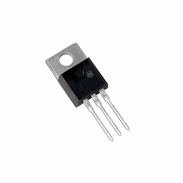
This Power MOSFET is designed to withstand high energy in the avalanche and commutation modes. The energy efficient design also offers a draintosource diode with a fast recovery time. Designed for low voltage, high speed switching applications in power converters and PWM motor controls, these devices are particularly well suited for bridge circuits where diode speed and commutating safe operating areas are critical and offer additional safety margin against unexpected voltage transients.
MTP20N15E Maximum Ratings
Rating
Symbol
Value
Unit
DrainSource Voltage
VDSS
150
Vdc
DrainGate Voltage (RGS = 1.0 MW)
VDGR
150
Vdc
GateSource Voltage Continuous NonRepetitive (tp 10 ms)
VGS VGSM
± 20 ± 32
Vdc
Drain Continuous Continuous @ 100°C Single Pulse (tp 10 ms)
ID ID IDM
20 12 60
Adc
Total Power Dissipation Derate above 25°C
PD
112 0.9
Watts W/°C
Operating and Storage Temperature Range
TJ, Tstg
55 to 150
°C
Single DraintoSource Avalanche Energy Starting TJ = 25°C (VDD = 120 Vdc, VGS = 10 Vdc, IL = 20 Apk, L = 0.3 mH)
EAS
60
mJ
Thermal Resistance Junction to Case Junction to Ambient
RqJC RqJA
1.1 62.5
°C/W
Maximum Lead Temperature for Soldering Purposes, 1/8, from case for 10 seconds
TL
260
°C
MTP20N15E Features
• Avalanche Energy Specified • SourcetoDrain Diode Recovery Time Comparable to a Discrete Fast Recovery Diode • Diode is Characterized for Use in Bridge Circuits • IDSS and VDS(on) Specified at Elevated Temperature
MTP20N20 General Description
This advanced TMOS EFET is designed to withstand high energy in the avalanche and commutation modes. The new energy efficient design also offers a draintosource diode with a fast recovery time. Designed for low voltage, high speed switching applications in power supplies, converters and PWM motor controls, these devices are particularly well suited for bridge circuits where diode speed and commutating safe operating areas are critical and offer additional safety margin against unexpected voltage transients.
MTP20N20 Maximum Ratings
Rating
Symbol
Value
Unit
DraintoSource Voltage
VDSS
200
Vdc
DraintoGate Voltage (RGS =1.0 M)
VDGR
200
Vdc
GatetoSource Voltage - Continuous - NonRepetitive (tp 10 ms)
VGS VGSM
± 20 ± 40
Vdc VPK
Drain Current - Continuous - Continuous@ 100°C - Single Pulse (tp 10 s)
ID ID IDM
20 12 60
Adc
Apk
Total Power Dissipation Derate above 25°C
PD
125 1.0
Watts W/°C
Operating and Storage Temperature Range
TJ, Tstg
55 to 150
°C
Single Pulse DraintoSource Avalanche Energy TJ = 25°C (VDD =50 Vdc, VGS =10Vdc,IL =20 Apk L =3.0mH, RG = 2.0
EAS
600
mJ
Thermal Resistance - Junction to Case - Junction to Ambient
RJC RJA
1.00 62.5
°C/W
Maximum Lead Temperature for Soldering Purposes, 1/8"from Case for 10 seconds
TL
260
°C
Designer's Data for "Worst Case" Conditions - The Designer's Data Sheet permits the design of most circuits entirely from the information presented. SOA Limit curves - representing boundaries on device characteristics - are given to facilitate "worst case" design.
EFET and Designer's are trademarks of Motorola, Inc. TMOS is a registered trademark of Motorola, Inc.
MTP20N20 Features
• Avalanche Energy Specified • SourcetoDrain Diode Recovery Time Comparable to a Discrete Fast Recovery Diode • Diode is Characterized for Use in Bridge Circuits • IDSS and VDS(on) Specified at Elevated Temperature
MTP20N20E General Description
This advanced TMOS EFET is designed to withstand high energy in the avalanche and commutation modes. The new energy efficient design also offers a draintosource diode with a fast recovery time. Designed for low voltage, high speed switching applications in power supplies, converters and PWM motor controls, these devices are particularly well suited for bridge circuits where diode speed and commutating safe operating areas are critical and offer additional safety margin against unexpected voltage transients. • Avalanche Energy Specified • SourcetoDrain Diode Recovery Time Comparable to a Discrete Fast Recovery Diode • Diode is Characterized for Use in Bridge Circuits • IDSS and VDS(on) Specified at Elevated Temperature
MTP20N20E Maximum Ratings
Rating
Symbol
Value
Unit
DrainSource Voltage
VGSS
200
Vdc
DrainGate Voltage (RGS = 1.0 M)
VDGR
200
Vdc
GateSource Voltage - Continuous - NonRepetitive (tp10ms)