
Power-Supply Circuits-Variable Output
Index
Regulator DC-DC Circuit and Pin of Power Supply Monitor and its Main Features-MAX624
Published:2011/9/13 3:01:00 Author:Zoey | Keyword: Regulator, DC-DC Circuit, Binary output Converter
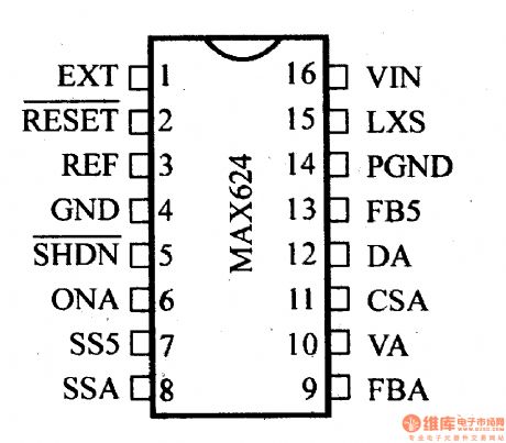
Switching frequency of MAX624 binary output DC-DC converter is 1MHz, working voltage range is 3.0~5.0V, static working current is 0.5mA, power-off current is 40µA. When the working turns to 5V, efficiency of SMPS will be 85%, input voltage 3V~5.5V, output voltage 5V±4%, output current 200mA, auxiliary output voltage 12V±2%. (View)
View full Circuit Diagram | Comments | Reading(858)
Regulator DC-DC Circuit and Pin of Power Supply Monitor and Linear Debugger
Published:2011/9/7 22:53:00 Author:Zoey | Keyword: Regulator, DC-DC Circuit, Linear Debugger
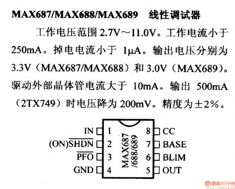
Working voltage range of MAX687/688/689 is 2.7V~11.0V. Its working current is below 250mA and power-off current is below 1µA. Output voltage of MAX676 and MAX688 is 3.3V, MAX689 is 3.0V. Current for driving external transistor should be larger than 10mA. Voltage will descend to 200mVwhen output currentreaches 500mA(2TX749). The accuracy is ±2%.
(View)
View full Circuit Diagram | Comments | Reading(879)
RECEIVER_IF_AMPLIFIER
Published:2009/7/17 2:46:00 Author:Jessie
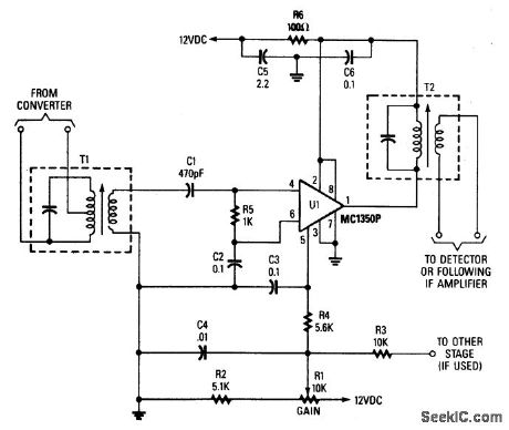
T1 is tuned to converter-output frequency U1 to provide 45-to-50-dB gain, depending on the design of T1 and T2. C2, C3, C4, CS, and C6 are bypass capacitors. R5 is a bias resistor. Gain is set by R1, which controls the voltage on pin 5 of U1. T1 and T2 should provide source and load impedance of 1-kΩ and 3-to 10 kΩ, respectively. R3 supplies dc bias to other stages, if required. (View)
View full Circuit Diagram | Comments | Reading(880)
75_watt_AF_power_amplifier_with_low_transient_intermodulation_distortion
Published:2009/7/20 5:16:00 Author:Jessie
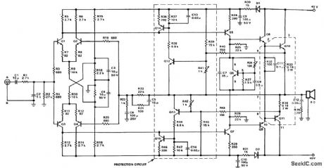
75-watt AF power amplifier with low-transient-intermodulation distortion (courtesy Fairchild Semiconductor). (View)
View full Circuit Diagram | Comments | Reading(1782)
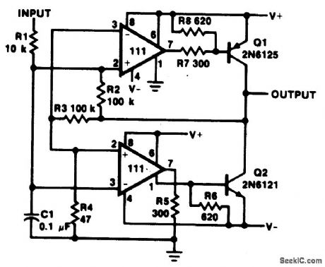
SWITCHING_POWER_AMPLIFIER
Published:2009/6/23 2:14:00 Author:May
View full Circuit Diagram | Comments | Reading(804)
Current Amplifier Circuit Diagram made up of LF356 and Others
Published:2011/6/14 19:24:00 Author:leo | Keyword: Current Amplifier Circuit Diagram, LF356
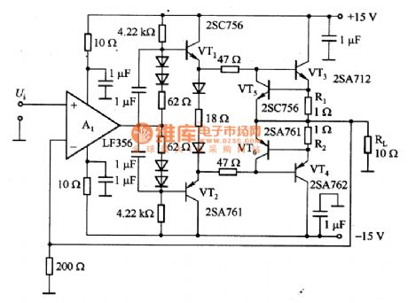
What the picture 1 shows is a current amplifier circuit made up of LF356 and so on. In the circuit, A1 is the backing amplifier while VT1 and VT2 (VT3 and VT4) can made up of the dual push-pull emitter follower circuit which amplifies DC signals with the frequency of 30 KHz and its output power is 1W. Vt5 and VT6 is used to protect power transistor when output circuit shorts. R1 is the sample and when the emitting polar current of VT3 and VT4 is 0.6A with the VT5 and VT6 on, VT5 and VT6 force the VT3 or VT4 to lower the base electric potential to protect the power transistor VT3 or VT4. (View)
View full Circuit Diagram | Comments | Reading(3637)
Mini UPS Circuit Digram
Published:2011/5/20 18:51:00 Author:leo | Keyword: Mini UPS Circuit Digram, LT1372
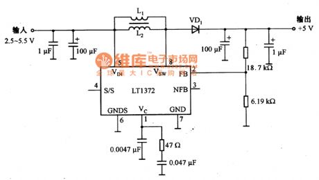
As what is shown in the picture, a and b are mini-UPS-circuits which are made up of quick charger circuit and main circuit. Picture 2(a) is quick charger circuit which use the way of quick charge to extend the life of the battery. The circuit made up of the operational amplifiers of A1 to A4 and related components manages the three working mode of the battery, which are charging, discharging and recharging. During charging the battery, it needs about 0.5A current and two to three hours. (View)
View full Circuit Diagram | Comments | Reading(2449)
Current Detection Circuit Diagram made up of LT1620 and Others
Published:2011/6/2 11:20:00 Author:leo | Keyword: Current Detection Circuit Diagram made up of LT1620 and Others, T1620
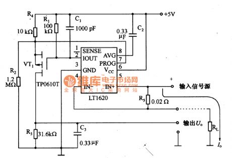
The picture shows a current detection circuit made up of LT1620 and so on. In this circuit, LT1620 is a integrated controller of voltage regulation power in the battery recharger. In the work mode, the LT1620 can produce load current signals under the +5V voltage.Itis madeup of a circuit with MOSFET(VT1) and other external devices to change the load current signals to output voltage based on the location. Therefore, the voltage can give a reflection of the change of load current I. (View)
View full Circuit Diagram | Comments | Reading(805)
UPS circuit with LM3524D
Published:2011/5/14 23:24:00 Author: | Keyword: LM3524D, UPS circuit
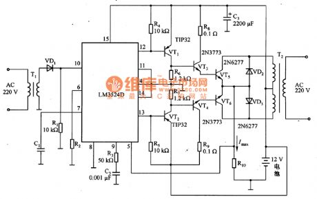
LM3524D is a kind of switch power supply controller which uses PWM operate mode. In the working mode, the pin 12 and pin 13 of LM3524D output pulse signals with the phase difference of 180°, whose voltages are amplified through VT1 and VT2 and then the electric currents are stimulated to be amplified by VT3 and VT4. As a result, both of the two processes drive the VT5 and VT6 to amplify the power of the pulse signals. The power amplifier VT5 and VT6 generates 12V square AV voltages on the one side of T2 transformer according to the alternating of the pulse signals outputting by VT1 and VT2.between turning on and turning off. After being stepped up, the square AV voltages are changed to 220 V AV voltages and are output through the other side of the transformer T2, which offer power supply for the load. The operating frequency of this circuit is decided by R2 and C1.VD2 and VD3 in this circuit is used to prevent the power amplifier from flowing through the current with a opposite direction. (View)
View full Circuit Diagram | Comments | Reading(3443)
MAX8819 Application Circuit
Published:2011/4/22 5:12:00 Author:Robert | Keyword: Application
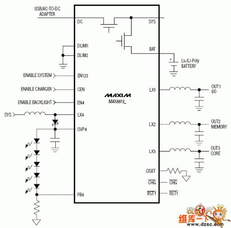
MAX8819 Application Circuit is shown below:
(View)
View full Circuit Diagram | Comments | Reading(656)
Circuit Categories
power supply circuit
Amplifier Circuit
Basic Circuit
LED and Light Circuit
Sensor Circuit
Signal Processing
Electrical Equipment Circuit
Control Circuit
Remote Control Circuit
A/D-D/A Converter Circuit
Audio Circuit
Measuring and Test Circuit
Communication Circuit
Computer-Related Circuit
555 Circuit
Automotive Circuit
Repairing Circuit