About SeekIC | Services | Payment | Advertisements service | Contact Us | Links
© 2008-2012 SeekIC.com Corp.All Rights Reserved.
Published:2011/4/6 3:15:00 Author:Nicole | Keyword: switching power supply, isolated | From:SeekIC
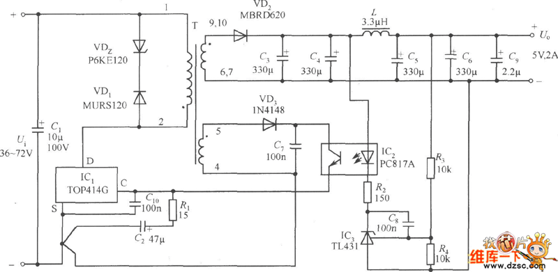
The circuit diagram as shown. C1 stands for the input filter capacitor. VDz and VD1 formonce sideclamp protection circuit. R1 is the resistance of the controlled end, C2 is a bypass capacitor. C10 is paralleled between TOP414GC-S-side to prevent high frequency interference occurring in the control side and caused power circuit malfunction. VD2 represents the output rectifier diodes, C3, C4, L, C5 and C6 form the output filter, C9 for the output Noise capacitor. External error amplifier is composed of the shunt regulator TL431. When the output voltage fluctuations, the samples obtained after R3, R4 partial pressure, compared with TL431 voltage reference, resulting in an external control signal, and then through the optical coupler PC817A to change TOP414G control terminal current, thereby regulating the track duty stabilize the Uo. Control loop gain is set by the R2. After VD3, C7 rectifier filter, the feedback winding voltage give the infrared receiver of PC817A power supply.
Reprinted Url Of This Article:
http://www.seekic.com/circuit_diagram/Power_Supply_Circuit/Switching-Regulator_Circuit/5V_2A_isolated_switching_power_supply_circuit_diagram.html
Print this Page | Comments | Reading(3)

Response in 12 hours
© 2008-2012 SeekIC.com Corp.All Rights Reserved.
Code: