
Circuit Diagram
Index 236
Voice controlling music lantern circuit (3)
Published:2012/12/18 2:01:00 Author:Ecco | Keyword: Voice controlling , music lantern
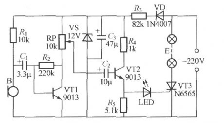
Transistor VT3 forms a main circuit of the lantern E, VT1 and VT2 form a control loop, the 220V AC is rectified by VD, Buck by R3, regulated by VS and filtered by C3 filter to output about 12V stable DC voltage for controlling the loop's power. Microphone B can pick up acoustic signal of indoor environment, then it convert it to electric signal which is amplified by the transistor VT1 level, then the amplified signal is flowing to the base of VT2 ( RP is a voice sensitivity adjustment potentiometer) by RP and C2. VT2 is connected into a non - biased emitter follower.
(View)
View full Circuit Diagram | Comments | Reading(1333)
INA321/322 amplifier circuit diagram using feedback capacitor to improve dynamic characteristics
Published:2012/12/18 1:48:00 Author:Ecco | Keyword: amplifier , feedback capacitor , improve, dynamic characteristics
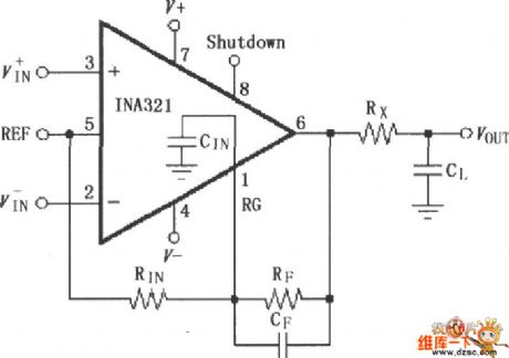
The both ends of the feedback resistor RF are connected to feedback capacitor CF in parallel, it is used to compensate for the feedback resistor, RG input equivalent capacitance and the effect on high - frequency signal from circuit board stray capacitance, so that the circuit has the best fast settling time. Output ( 6 feet ) end is connected to Rx, CL to reduce high-frequency noise, CIN is equal to INA321/322 input capacitance ( 3pF) and stray capacitance. RIN · CIN = RF · CF.
(View)
View full Circuit Diagram | Comments | Reading(1239)
Basic connection diagram of INA326/327 signal and power
Published:2012/12/18 1:38:00 Author:Ecco | Keyword: Basic connection, signal , power
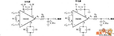
It selects most accurate 0.1μF capacitor for the power supply filtering, and it should be placed as close as possible to the chip power pin. Ro, Co are an output filters which can filter the output noise of circuit; at the same time, it can be used as the input filter for next-stage circuit, such as an input filter of analog - digital converter. The output voltage is based on the ground terminal of R2 / / C2 basis.
(View)
View full Circuit Diagram | Comments | Reading(1213)
Tracking 0 ~ ± 15V regulator circuit diagram
Published:2012/12/18 0:30:00 Author:Ecco | Keyword: Tracking, 0 ~ ± 15V, regulator
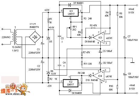
Working principle: the whole circuit is shown as the figure. The power input part is a common transformer buck bridge rectifier, increasing the capacitor filter can get ± 22V DC symmetrical voltage. Another two ± 6.8V auxiliary voltagea are also derived to add on IC4 and op amp IC3's V + and V-terminals to ensure that IC3 and IC4 working voltage does not exceed the limits.
(View)
View full Circuit Diagram | Comments | Reading(5173)
Homemade eight-block digital regulated power supply circuit diagram
Published:2012/12/18 0:23:00 Author:Ecco | Keyword: Homemade, eight-block, digital, regulated power supply
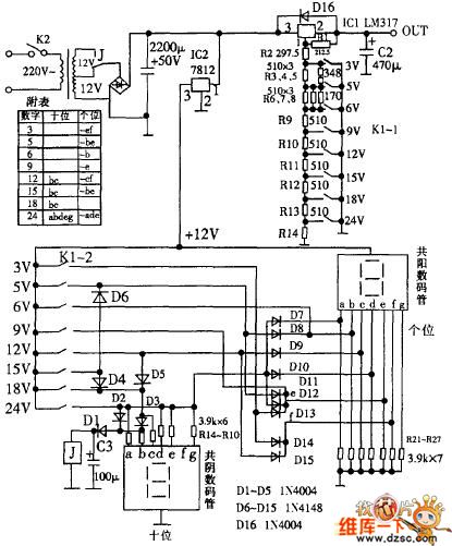
The circuit is divided into two parts, one part is the regulator circuit, the other part is a digital decoder circuit. Integrated regulator block is based on LM317 adjustable regulator to matched with the corresponding partial pressure resistor, then it can get eight blocks of voltage outputs. In order to reduce the power consumption of LM317, transformer uses the center tap. When the output voltage is below 9V, it uses 12V AC voltage; When the output voltage is above 12V, it uses 24V AC voltage, and the voltage is automatically switched by relay.
(View)
View full Circuit Diagram | Comments | Reading(1812)
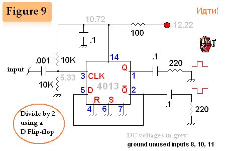
D Flip-Flop with dual or single output.
Published:2012/12/17 20:37:00 Author:muriel | Keyword: D Flip-Flop, dual or single output.
View full Circuit Diagram | Comments | Reading(1285)
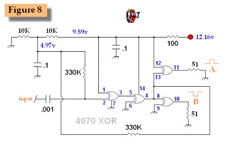
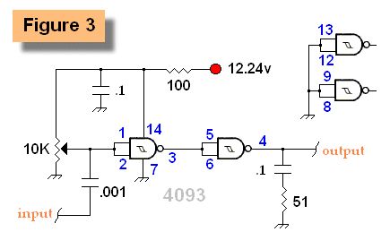
"popcorn" XOR output balancer
Published:2012/12/17 20:36:00 Author:muriel | Keyword: "popcorn" XOR , output balancer
View full Circuit Diagram | Comments | Reading(656)
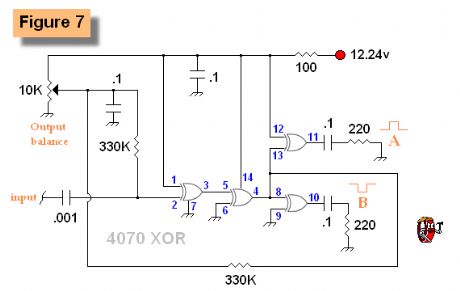
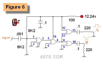
Exclusive-OR gates with split output 2
Published:2012/12/17 20:35:00 Author:muriel | Keyword: Exclusive-OR gates , split output
View full Circuit Diagram | Comments | Reading(600)
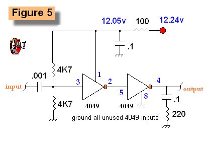
Exclusive-OR gates with split output
Published:2012/12/17 20:35:00 Author:muriel | Keyword: Exclusive-OR gates , split output
View full Circuit Diagram | Comments | Reading(662)
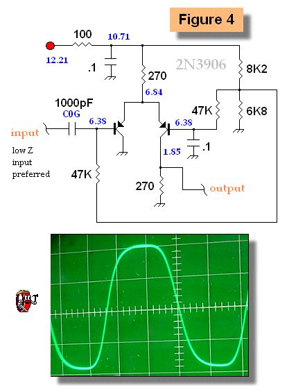
an inverter which was connected to the output of the differential amp
Published:2012/12/17 20:34:00 Author:muriel | Keyword: inverter, differential amp
View full Circuit Diagram | Comments | Reading(754)
symmetrical AC waveform
Published:2012/12/17 20:33:00 Author:muriel | Keyword: symmetrical AC waveform
View full Circuit Diagram | Comments | Reading(712)
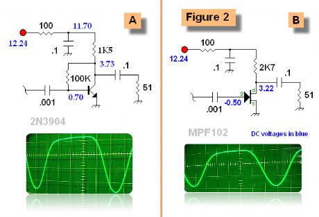
JFET switch (B) output waveform
Published:2012/12/17 20:32:00 Author:muriel | Keyword: JFET switch (B), output waveform
View full Circuit Diagram | Comments | Reading(914)
Shaping a Sine Wave Into a Square Wave
Published:2012/12/17 20:32:00 Author:muriel | Keyword: Sine Wave, Square Wave
View full Circuit Diagram | Comments | Reading(1093)
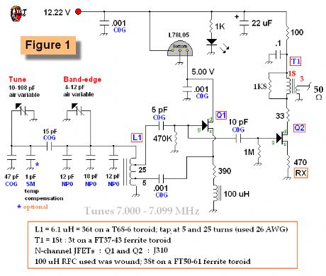
Base VFO
Published:2012/12/17 20:31:00 Author:muriel | Keyword: Base VFO
View full Circuit Diagram | Comments | Reading(1281)
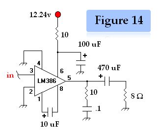
LM386 Power Experiments
Published:2012/12/17 20:28:00 Author:muriel | Keyword: LM386 , Power Experiments
View full Circuit Diagram | Comments | Reading(873)
One KHz Low Distortion Signal Generator
Published:2012/12/17 20:28:00 Author:muriel | Keyword: One KHz , Low Distortion , Signal Generator

View full Circuit Diagram | Comments | Reading(2150)
One KHz Digital and Analog Oscillator 2
Published:2012/12/17 20:27:00 Author:muriel | Keyword: One KHz, Digital and Analog , Oscillator
View full Circuit Diagram | Comments | Reading(713)
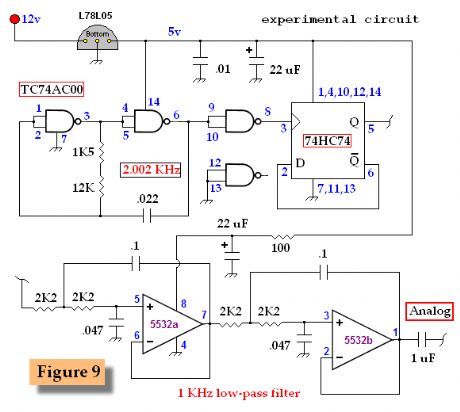
One KHz Digital and Analog Oscillator
Published:2012/12/17 20:26:00 Author:muriel | Keyword: One KHz, Digital and Analog, Oscillator
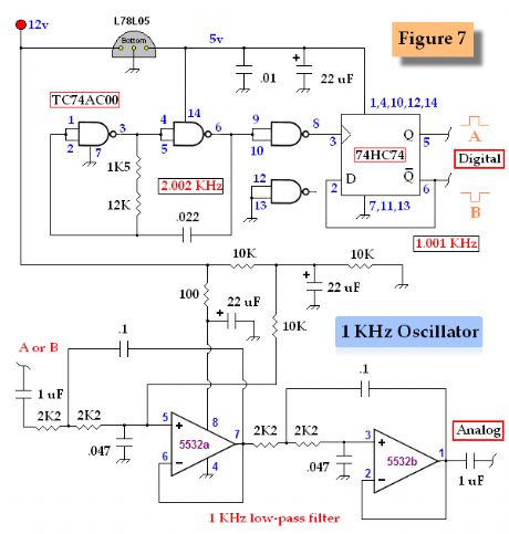
View full Circuit Diagram | Comments | Reading(914)
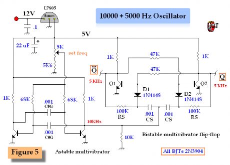
10000 and 5000 Hz Multivibrator Clock
Published:2012/12/17 20:26:00 Author:muriel | Keyword: 10000 and 5000 Hz, Multivibrator Clock
View full Circuit Diagram | Comments | Reading(855)
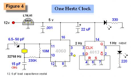
One Hertz Precision Time Base
Published:2012/12/17 20:25:00 Author:muriel | Keyword: One Hertz , Precision Time Base
View full Circuit Diagram | Comments | Reading(1413)
| Pages:236/2234 At 20221222223224225226227228229230231232233234235236237238239240Under 20 |
Circuit Categories
power supply circuit
Amplifier Circuit
Basic Circuit
LED and Light Circuit
Sensor Circuit
Signal Processing
Electrical Equipment Circuit
Control Circuit
Remote Control Circuit
A/D-D/A Converter Circuit
Audio Circuit
Measuring and Test Circuit
Communication Circuit
Computer-Related Circuit
555 Circuit
Automotive Circuit
Repairing Circuit