
Circuit Diagram
Index 402
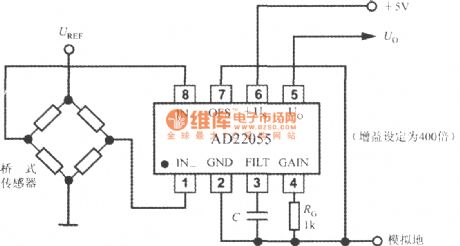
The typical application circuit of bridge sensor signal amplifier AD22055
Published:2011/12/1 1:45:00 Author:Ecco | Keyword: typical application , bridge sensor , signal amplifier
View full Circuit Diagram | Comments | Reading(623)
The simple application circuit of impedance humidity sensor
Published:2011/12/1 1:42:00 Author:Ecco | Keyword: simple application , impedance humidity sensor
View full Circuit Diagram | Comments | Reading(1310)
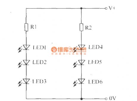
The driver with many LEDs
Published:2011/11/30 1:03:00 Author:Ecco | Keyword: driver , many LEDs
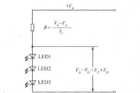
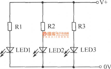
The LEDs connected in series isonly driven bya current limitedresistor:
The circuit can drive the LEDs in any quantity:
The LEDs connected in parallel can drive many LEDs:
(View)
View full Circuit Diagram | Comments | Reading(642)
The monostable circuit composed of optical coupler
Published:2011/11/30 1:24:00 Author:Ecco | Keyword: monostable circuit , optical coupler
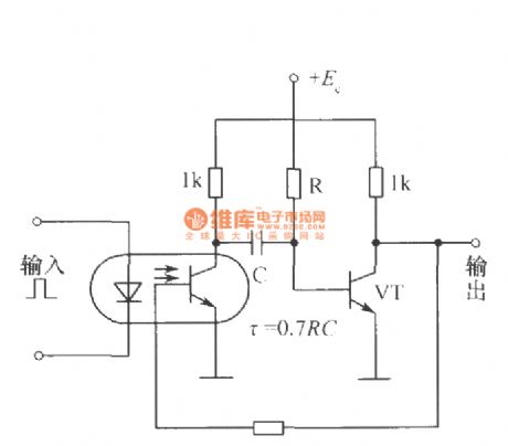
View full Circuit Diagram | Comments | Reading(914)
The internal half-bridge network strain gauge circuit using broadband response signal conditioner 1B31
Published:2011/12/1 1:44:00 Author:Ecco | Keyword: internal , half-bridge network, strain gauge , broadband, response signal conditioner
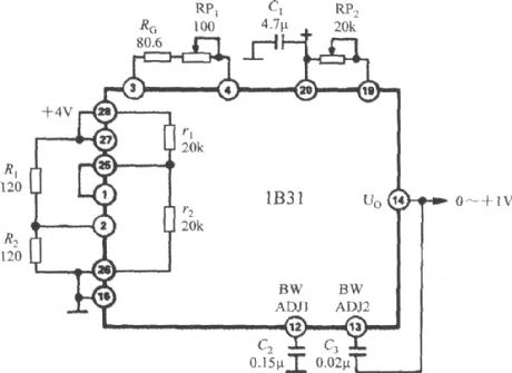
View full Circuit Diagram | Comments | Reading(1230)
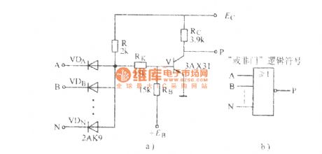
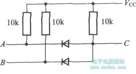
Diode OR gate circuit
Published:2011/12/5 20:58:00 Author:Ecco | Keyword: Diode, OR gate
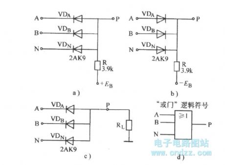
The circuit shown in Figure a is used for positive logic system, and it is known as positive orgate.The circuit shown in Figure b is used for the negative logic system , and it iscalled the negative or gate.
The gate circuit with omissiongate resistor is shown in Figure c .Figure dshows the or gate logic symbols.
(View)
View full Circuit Diagram | Comments | Reading(1996)
Diode AND gate decoder circuit (2)
Published:2011/12/5 1:52:00 Author:Ecco | Keyword: Diode , AND gate, decoder

View full Circuit Diagram | Comments | Reading(869)
Diode and gate circuit
Published:2011/12/5 1:51:00 Author:Ecco | Keyword: Diode, gate
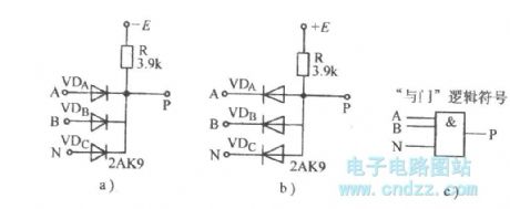
a) is used for positive logic , and it is called asthe positive AND gate.
b) is used for negative logic , and it is called the negative AND gate.c)is and gate logic symbol.
(View)
View full Circuit Diagram | Comments | Reading(1408)
Diode - transistor NOR gate
Published:2011/12/5 20:52:00 Author:Ecco | Keyword: Diode, transistor , NOR gate
a)shows thediode - transistor NOR gate circuit .b)shows the logical symbols.
(View)
View full Circuit Diagram | Comments | Reading(1154)
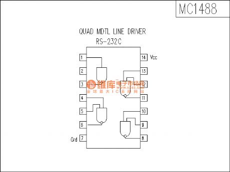
MC1488 circuit
Published:2011/12/5 1:59:00 Author:Ecco
View full Circuit Diagram | Comments | Reading(858)
Half-adder circuit
Published:2011/12/5 1:59:00 Author:Ecco | Keyword: Half-adder
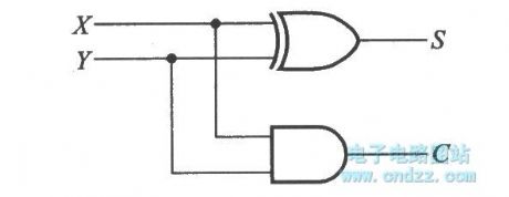
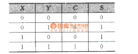
The valuetable:
(View)
View full Circuit Diagram | Comments | Reading(1182)
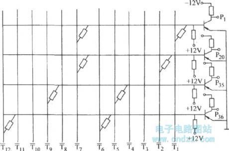
Shifting digit picking machine
Published:2011/12/5 1:58:00 Author:Ecco | Keyword: Shifting, digit picking machine
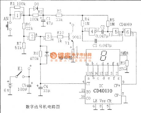
The figure is the analog color ball random selection device.
(View)
View full Circuit Diagram | Comments | Reading(569)
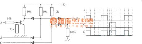
The logic circuit composed of diodes and transistors and its operation waveforms
Published:2011/12/5 1:55:00 Author:Ecco | Keyword: logic circuit , operation waveforms , diodes , transistors
View full Circuit Diagram | Comments | Reading(596)
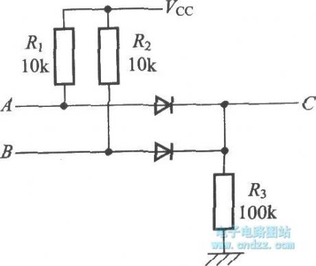
The OR circuit C = A + B composed of diode and resistor
Published:2011/12/5 1:53:00 Author:Ecco | Keyword: OR circuit , C = A + B , diode , resistor
View full Circuit Diagram | Comments | Reading(720)
The AND circuit C = A · B composed of diodes and resistors
Published:2011/12/5 2:02:00 Author:Ecco | Keyword: AND circuit, C = A · B , diodes , resistors
View full Circuit Diagram | Comments | Reading(630)
OR NOT gate circuit
Published:2011/12/5 2:07:00 Author:Ecco | Keyword: OR NOT gate
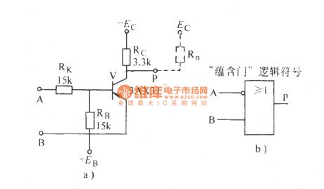
The transistor's emitter is used as the gate circuit of input gate, and it is known as the OR NOT gate, and it isshown in Figure a) . b)shows its logic symbols.
(View)
View full Circuit Diagram | Comments | Reading(1035)
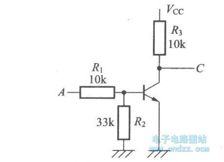
The NOT circuit using transistors
Published:2011/12/5 2:02:00 Author:Ecco | Keyword: NOT circuit , transistors
View full Circuit Diagram | Comments | Reading(691)
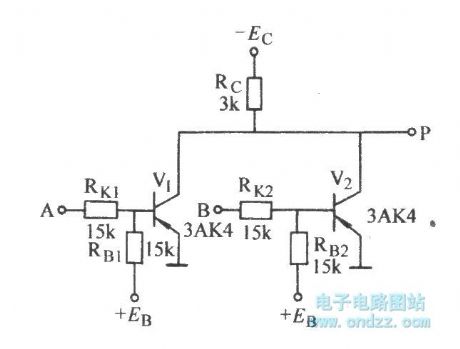
The transistor NOR gate circuit with two input ends
Published:2011/12/5 2:33:00 Author:Ecco | Keyword: transistor , NOR gate , two input ends
View full Circuit Diagram | Comments | Reading(1152)
The transistor NOR gate circuit with resistance on two input ends
Published:2011/12/5 2:32:00 Author:Ecco | Keyword: transistor , NOR gate , resistance , two input ends
View full Circuit Diagram | Comments | Reading(716)
The NOT gate circuit clamping by Zener diode
Published:2011/12/5 2:30:00 Author:Ecco | Keyword: NOT gate, clamping, Zener diode
View full Circuit Diagram | Comments | Reading(1393)
| Pages:402/2234 At 20401402403404405406407408409410411412413414415416417418419420Under 20 |
Circuit Categories
power supply circuit
Amplifier Circuit
Basic Circuit
LED and Light Circuit
Sensor Circuit
Signal Processing
Electrical Equipment Circuit
Control Circuit
Remote Control Circuit
A/D-D/A Converter Circuit
Audio Circuit
Measuring and Test Circuit
Communication Circuit
Computer-Related Circuit
555 Circuit
Automotive Circuit
Repairing Circuit