Position: Home > Circuit Diagram > Measuring and Test Circuit > The bilateral band modem circuit composed of NE561B
Measuring and Test Circuit
The bilateral band modem circuit composed of NE561B
Published:2011/6/16 20:55:00 Author:qqtang | Keyword: bilateral band, modem circuit | From:SeekIC
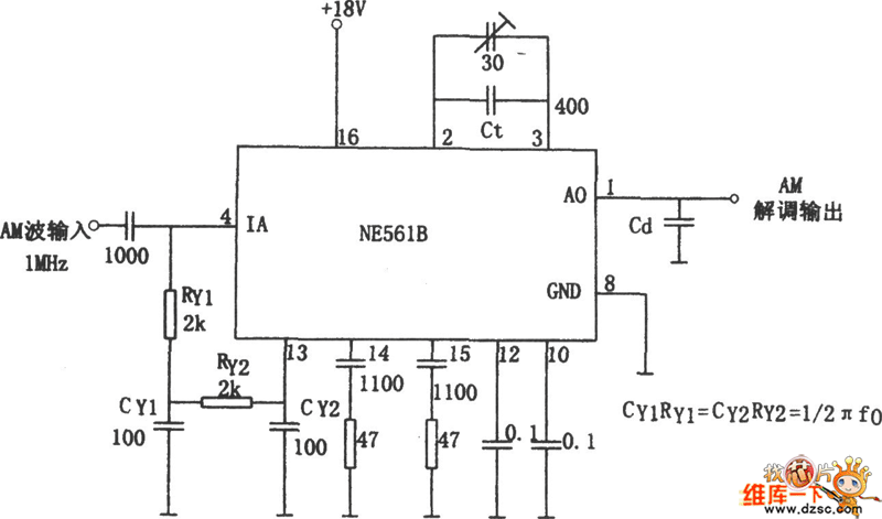
In the figure is the bilateral band modem circuit composed of NE561B. The loading frequency of the input modulating signal is f0=1MHz. When the AM modulation signal is added on the input terminal of the multiplier, it is also added on the phase detection circuit by Rv1, CY1, Y2 and CY2, and it sets the VCO frequency of PLL at f0.
Reprinted Url Of This Article:
http://www.seekic.com/circuit_diagram/measuring_and_test_circuit/the_bilateral_band_modem_circuit_composed_of_ne561b.html
Print this Page | Comments | Reading(3)

Article Categories
power supply circuit
Amplifier Circuit
Basic Circuit
LED and Light Circuit
Sensor Circuit
Signal Processing
Electrical Equipment Circuit
Control Circuit
Remote Control Circuit
A/D-D/A Converter Circuit
Audio Circuit
Measuring and Test Circuit
Communication Circuit
Computer-Related Circuit
555 Circuit
Automotive Circuit
Repairing Circuit
Code: