Features: • AV9172-07 input is 66 MHz with 66 and 33 MHz output buffers• AV9172-01 is pin compatible with Gazelle GA1210E• ±250ps skew (max) between outputs• ±500ps skew (max) between input and outputs• Input frequency range from 10 MHz to 50 MHz (-01, -03) and from 2...
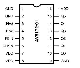
AV9172: Features: • AV9172-07 input is 66 MHz with 66 and 33 MHz output buffers• AV9172-01 is pin compatible with Gazelle GA1210E• ±250ps skew (max) between outputs• ±500ps skew (max...
SeekIC Buyer Protection PLUS - newly updated for 2013!
268 Transactions
All payment methods are secure and covered by SeekIC Buyer Protection PLUS.
Features: SpecificationsDescriptionThe AV9107C-07 is a kind of CPU frequency generator.There are s...
The AV9172 is designed to generate low skew clocks for clock distribution in high-performance PCs and workstations. It uses phase-locked loop technology to align the phase and frequency of the output clocks with an input reference clock. Because the input to output skew is guaranteed to ±500ps, the part acts as a "zero delay" buffer.
The AV9172 has six configurable outputs. The AV9172-01 version has one output that runs at the same phase and frequency as the reference clock. A second output runs at the same frequency as the reference, but can either be in phase or 180° out of phase from the input clock. Two outputs are provided that are at twice the reference frequency and in phase with the reference clock. The final outputs can be programmed to be replicas of the 2x clocks or non-overlapping two phase clocks at twice the reference frequency. The AV9172-01 and AV9172-03 operates with input clocks from 10 MHz to 50 MHz while producing outputs from 10 MHz to 100 MHz. The AV9172-07 operates with input clocks from 20 to 100 MHz.
The use of a phase-locked loop (PLL) allows the output clocks to run at multiples of the input clock. This permits routing of a lower speed clock and local generation of a required high speed clock. Synchronization of the phase relationship between the input clock and the output clocks is accomplished when one output clock is connected to the input pin FBIN. The PLL circuitry matches rising edges of the input clock and output clocks.