BS616LV2011

Features: • Very low operation voltage : 2.4 ~ 5.5V• Very low power consumption : Vcc = 3.0V C-grade: 20mA (Max.) operating current I-grade: 25mA (Max.) operating current 0.1uA (Typ.) CMOS standby current Vcc = 5.0V C-grade: 40mA (Max.) operating current I -grade: 45mA (Max.) operating...

product image

BS616LV2011 Picture
SeekIC No. : 004301815 Detail

BS616LV2011: Features: • Very low operation voltage : 2.4 ~ 5.5V• Very low power consumption : Vcc = 3.0V C-grade: 20mA (Max.) operating current I-grade: 25mA (Max.) operating current 0.1uA (Typ.) CM...

floor Price/Ceiling Price

Part Number:
BS616LV2011
Supply Ability:
5000

Price Break

  • Qty
  • 1~5000
  • Unit Price
  • Negotiable
  • Processing time
  • 15 Days
Total Cost: $ 0.00

SeekIC Buyer Protection PLUS - newly updated for 2013!

  • Escrow Protection.
  • Guaranteed refunds.
  • Secure payments.
  • Learn more >>

Month Sales

268 Transactions

Rating

evaluate  (4.8 stars)

Upload time: 2024/3/27

Payment Methods

All payment methods are secure and covered by SeekIC Buyer Protection PLUS.

Notice: When you place an order, your payment is made to SeekIC and not to your seller. SeekIC only pays the seller after confirming you have received your order. We will also never share your payment details with your seller.
Product Details

Description


Features:

• Very low operation voltage : 2.4 ~ 5.5V
• Very low power consumption :
   Vcc = 3.0V C-grade: 20mA (Max.) operating current
   I-grade: 25mA (Max.) operating current
   0.1uA (Typ.) CMOS standby current
   Vcc = 5.0V C-grade: 40mA (Max.) operating current
   I -grade: 45mA (Max.) operating current
   0.6uA (Typ.) CMOS standby current
• High speed access time :
   -70 70ns (Max.) at Vcc = 3.0V
   -10 100ns (Max.) at Vcc = 3.0V
• Automatic power down when chip is deselected
• Three state outputs and TTL compatible
• Fully static operation
• Data retention supply voltage as low as 1.5V
• Easy expansion with CE and OE options
• I/O Configuration x8/x16 selectable by LB and UB pin


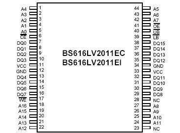
Pinout

  Connection Diagram


Specifications

SYMBOL PARAMETER RATING UNITS
VTERM Terminal Voltage with
Respect to GND
-0.5 to
Vcc+0.5
V
TBIAS Temperature Under Bias -40 to +85
TSTG Storage Temperature -60 to +150
PT Power Dissipation 1.0 W
IOUT DC Output Current 20 mA

1. Stresses greater than those listed under ABSOLUTE MAXIMUM RATINGS may cause permanent damage to the device. This is a stress rating only and functional operation of the device at these or any other conditions above those indicated in the operational sections of this specification is not implied. Exposure to absolute maximum rating conditions for extended periods may affect reliability.


Description

The BS616LV2011 is a high performance, very low power CMOS Static Random Access Memory organized as 131,072 words by 16 bits and operates from a wide range of 2.4V to 5.5V supply voltage. Advanced CMOS technology and circuit techniques provide both high speed and low power features of BS616LV2011 with a typical CMOS standby current of 0.1uA and maximum access time of 70/100ns in 3V operation. Easy memory expansion is provided by an active LOW chip enable(CE), active LOW output enable(OE) and three-state output drivers.

The BS616LV2011 has an automatic power down feature, reducing the power consumption significantly when chip is deselected. The BS616LV2011 is available in DICE form, JEDEC standard 44-pin TSOP Type II package , JEDEC standard 48-pin TSOP Type I package and 48-ball BGA package.


Customers Who Bought This Item Also Bought

Margin,quality,low-cost products with low minimum orders. Secure your online payments with SeekIC Buyer Protection.
Line Protection, Backups
Hardware, Fasteners, Accessories
Inductors, Coils, Chokes
Fans, Thermal Management
Power Supplies - External/Internal (Off-Board)
View more