Series: -
Number of Converters: 1
Mounting Type: Surface Mount
Number of Inputs and Type: 1 Single-Ended, Unipolar
Voltage Supply Source: Analog and Digital
Operating Temperature: -40°C ~ 85°C
Number of Bits: 8
Packaging: Tube
Sampling Rate (Per Second): 20M
Data Interface: Parallel
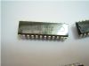
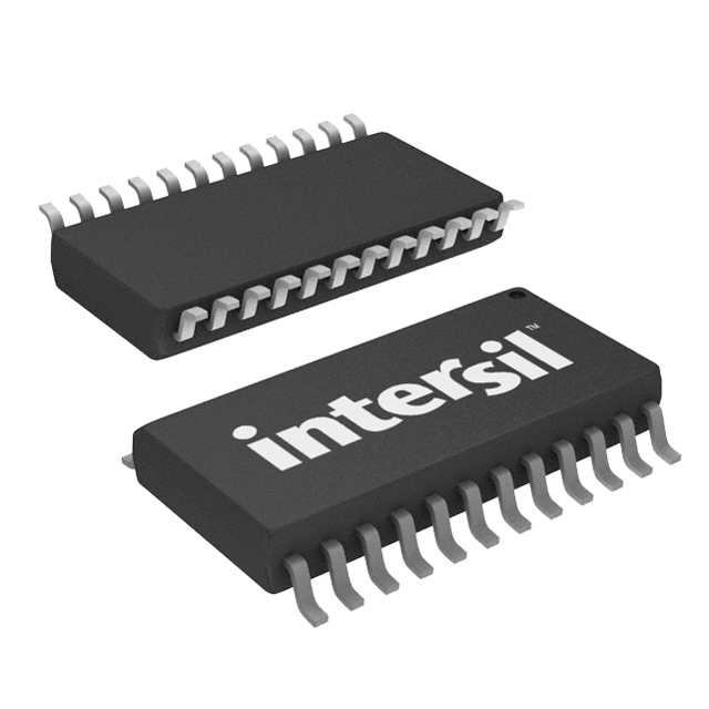
Package / Case: 24-SOIC (0.209", 5.30mm Width)
Power Dissipation (Max): 60mW
Supplier Device Package: 24-SOIC W
Manufacturer: Intersil
Features: • Resolution . . . . . . . . . . . . . . . . . . . . 8-Bit ±0.3 LSB (DNL)
• Maximum Sampling Frequency . . . . . . . . . . . . . . 20MSPS
• Low Power Consumption . . . . . . 60mW (at 20MSPS Typ) (Reference Current Excluded)
• Built-In Sample and Hold Circuit
• Built-In Reference Voltage Self Bias Circuit
• Three-State TTL Compatible Output
• Single +5V Power Supply
• Low Input Capacitance. . . . . . . . . . . . . . . . . . . 11pF (Typ)
• Reference Impedance . . . . . . . . . . . . . . . . . . . 300 (Typ)
• Evaluation Board Available (HI1175-EV)
• Low Cost
• Direct Replacement for the Sony CXD1175Application• Video Digitizing
• PC Video Capture
• Image Scanners
• TV Set Top Boxes
• Multimedia
• Personal Communication Systems (PCS)Pinout SpecificationsSupply Voltage, VDD . . . . . . . . . . . . . . . . . . . . . . . . . . . . . . . . ..7V
Reference Voltage, VRT, VRB . . . . . . . . . . . . . . . . . . . . VDD to VSS
Analog Input Voltage, VIN . . . . . . . . . . . . . . . . . . . . . . VDD to VSS
Digital Input Voltage, CLK . . . . . . . . . . . . . . . . . . . . . . VDD to VSS
Digital Output Voltage, VOH, VOL . . . . . . . . . . . . . . . . . VDD to VSSDescriptionThe HI1175 is an 8-bit, analog-to-digital converter built in a 1.4m CMOS process. The low power, low differential gain and phase, high sampling rate, and single 5V supply make the HI1175 ideal for video and imaging applications.
The adoption of a 2-step flash architecture achieves low power consumption (60mW) at a maximum conversion speed of 20MSPS (Min), 35MSPS typical with only a 2.5 clock cycle data latency. The HI1175 also features digital output enable/disable and a built in voltage reference. The HI1175 can be configured to use the internal reference or an external reference if higher precision is required.
Parameters: | Technical/Catalog Information | HI1175JCB |
| Vendor | Intersil |
| Category | Integrated Circuits (ICs) |
| Number of Bits | 8 |
| Package / Case | 24-SOIC (7.5mm Width) |
| Data Interface | Parallel |
| Packaging | Tube |
| Sampling Rate (Per Second) | 20M |
| Operating Temperature | -40°C ~ 85°C |
| Voltage Supply Source | Analog and Digital |
| Number of Inputs and Type | 1 Single-Ended, Unipolar |
| Number of Converters | 1 |
| Power Dissipation (Max) | 60mW |
| Lead Free Status | Lead Free |
| RoHS Status | RoHS Compliant |
| Other Names | HI1175JCB
HI1175JCB
|
 HI1175JCB Data Sheet