Features: ` Fast Access Times: 17/20/25/35 ns
` Wide Word (18-Bits) for:
Improved Performance
Reduced Component Count
Nine-bit Byte for Parity
` Transparent Address Latch
` Reduced Loading on Address Bus
` Low-Power Stand-by Mode when Deselected
` TTL Compatible I/O
` 5 V ± 10% Supply
` 2 V Data Retention
` JEDEC Standard Pinout
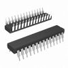
` Package: 52-Pin PLCC
Pinout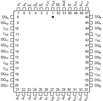 Specifications
| PARAMETER |
RATING |
| VCC to VSS Potential |
0.5 V to 7 V |
| Input Voltage Range |
0.5 V to VCC + 0.5 V |
| DC Output Current 2 |
± 40 mA |
| Storage Temperature Range |
65 to 150 |
| Power Dissipation (Package Limit) |
2 W |
NOTES:
1. Stresses greater than those listed under 'Absolute Maximum Ratings' may cause permanent damage to the device. This is a stress rating for transient conditions only. Functional operation of the device at these or any other conditions above those indicated in the 'Operating Range' of this specification is not implied. Exposure to absolute maximum rating conditions for extended periods may affect reliability.
2. Outputs should not be shorted for more than 30 seconds. No more than one output should be shorted at any time.
DescriptionThe LH521028 is a high-speed 1,179,648-bit CMOS SRAM organized as 64K ´ 18. A fast, efficient design is obtained with a CMOS periphery and a matrix constructed with polysilicon load memory cells. The LH521028 is available in a compact 52-Pin PLCC, which along with the six pairs of supply terminals, provide for reliable operation.
The control signals include Write Enable (W), Chip Enable (E), High and Low Byte Select (SL and SH), Output Enable (G) and Address Latch Enable (ALE). The wide word provides for reduced component count, improved density, reduced Address bus loading and improved performance. The wide word also allows for byte-parity with no additional RAM required.
This RAM is fully static in operation. The Chip Enable (E) control permits Read and Write operations when active (LOW) or places the RAM in a low-power standby mode when inactive (HIGH).The Byte-select controls, SH and SL, are also used to enable or disable Read and Write operations on the high and the low bytes. The Address Latches are transparent when ALE is HIGH (for applications not requiring a latch), and are latched when ALE is LOW. The Address Latches and the wide word help to eliminate the need for external Address bus buffers and/or latches.
Write cycles occur when Chip Enable (E), SH and/or SL, and Write Enable (W) are LOW. The Byte-select signals can be used for Byte-write operations by disabling the other byte during the Write operation. Data is transferred from the DQ pins to the memory location specified by the 16 address lines. The proper use of the Output Enable control (G) can prevent bus contention.
When E and either SH or SL are LOW and W is HIGH, a static Read will occur at the memory location specified by the address lines. G must be brought LOW to enable the outputs. Since the device is fully static in operation, new Read cycles can be performed by simply changing the address with ALE HIGH.

 LH521028 Data Sheet