DescriptionThe MMFT5P03HDT3 is a kind of power MOSFET. The device is capable of withstanding high energy in the avalanche and commutation modes and the drain-to-source diode has a very low reverse recovery time. The device is intended for use in low voltage, high speed switching applications where power efficiency is concerned. The typical applications include dcdc converters, and power management in portable and battery powered products such as computers, printers, cellular and cordless phones. In addition, the device is suitable for low voltage motor controls in mass storage products such as disk drives and tape drives.
There are some features of MMFT5P03HDT3 as follows: (1)ultra low RDS(on) provides higher efficiency and extends battery life; (2)logic level gate drive: can be driven by logic ics; (3)miniature sot23 surface mount package: saves board space; (4)diode is characterized for use in bridge circuits; (5)diode exhibits high speed, with soft recovery; (6)idss specified at elevated temperature; (7)avalanche energy specified.
The following is about the MMFT5P03HDT3 maximum ratings (TJ=25 unless otherwise noted): (1)drain-to-ource voltage, VDSS: 30 V; (2)drain-to-gate voltage (RGS=1.0 M), VDGR: 30 V; (3)gate-to-source voltage, continuous, VGS: ±20 V; (4)operating and storage temperature range, TJ, TSTG: -55 to 150; (5)single pulse draintosource avalanche energy -starting TJ=25, EAS: 250 mJ at VDD=30 Vdc, VGS=10 Vdc, Peak IL=12 Apk, L=3.5 mH, RG=25. Then is about the maximum ratings (1"SQ. FR-4 or G-10 PCB, 10 seconds): (1)thermal resistance-junction to ambient, RTHJA: 40/W; (2)total power dissipation @ TA=25, PD: 3.13 W; (3)drain current-continuous @ TA=25, ID: 5.2 A and 4.1 A at TA=70; (4)pulsed drain current, IDM: 26 A. The last one is about the maximum ratings (minimum, FR-4 or G-10 PCB, 10 seconds): (1)thermal resistance-junction to ambient, RTHJA: 80/W; (2)total power dissipation @ TA=25, PD: 1.56 W; (3)drain current-continuous @ TA=25, ID: 3.7 A and 2.9 A at TA=70; (4)pulsed drain current, IDM: 19 A.

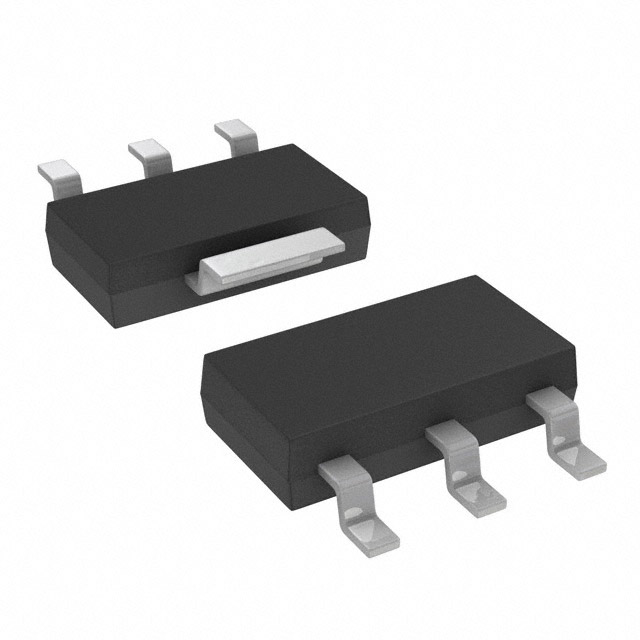
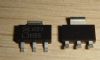
 MMFT5P03HDT3 Data Sheet