DescriptionThe S1T8602B01-D0B0 is designed as a audio power amplifier available for low voltages. It supplies differential outputs for maximizing output swing at low voltages. It doesn't need coupling capacitors to the speaker. The gain of this amp is controlled easily by two external resistors.S1...
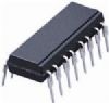
S1T8602B01-D0B0: DescriptionThe S1T8602B01-D0B0 is designed as a audio power amplifier available for low voltages. It supplies differential outputs for maximizing output swing at low voltages. It doesn't need coupli...
SeekIC Buyer Protection PLUS - newly updated for 2013!
268 Transactions
All payment methods are secure and covered by SeekIC Buyer Protection PLUS.
The S1T8602B01-D0B0 is designed as a audio power amplifier available for low voltages. It supplies differential outputs for maximizing output swing at low voltages. It doesn't need coupling capacitors to the speaker. The gain of this amp is controlled easily by two external resistors.
S1T8602B01-D0B0 has eight features. (1)Wide supply voltage (2 to 16V). (2)Low quiescent supply current (Icc=2.7mA typ). (3)Easy gain control. (4)Medium output power would be Po=250mW at Vcc=6V and Rl=32W and THD=10%. (5)Minimum external parts. (6)Various load impedance range (8W to 100W). (7)Low distortion. (8)Mute function (lcc=65mA typ). Those are all the main features.
Some absolute maximum ratings of S1T8602B01-D0B0 have been concluded into several points as follow. (1)Its supply voltage would be from -1.0V to +18V. (2)Its output current (output pin) would be +/-250mA. (3)Its maximum voltage (input, ripple rejection, mute pin) would be from -1.0V to Vcc+1.0V. (4)Its applied output voltage (output pin) when disabled would be from -1.0V to Vcc+1.0V. (5)Its junction temperature range would be from -55°C to 140°C. It should be noted that stresses above those listed in absolute maximum ratings may cause permanent damage to device.
Also some electrical characteristics of S1T8602B01-D0B0 are concluded as follow. (1)Its operating current (RL=0) would be typ 2.7mA and max 4.0mA with conditions of Vcc=3.0V and mute=0.8V and would be typ 3.3mA and max 5.0mA with conditions of Vcc=16V and mute=0.8V. (2)Its output voltage output pin would be min 1.0V and typ 1.15V and max 1.25V at Vcc=3.0V and would be typ 2.65V at Vcc=6.0V and would be typ 5.65V at Vcc=12V. (3)Its output offset voltage would be min -30mV and typ 0mV and max +30mV. (4)Its output high level would be typ Vcc-1.0V and output low level would be typ 0.16V. And so on. If you have any question or suggestion or want to know more information please contact us for details. Thank you!